|
数据搜索系统,热门电子元器件搜索 |
|
|
数据搜索系统,热门电子元器件搜索 |
|
AD604ARSZ-R7 数据表(PDF) 16 Page - Analog Devices |
|
|
|||||||||||||||||||||||||||||
AD604ARSZ-R7 数据表(HTML) 16 Page - Analog Devices |
|
|
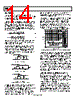
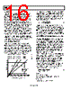
16 / 32 page  AD604 Rev. D | Page 16 of 32 AC COUPLING The DSX portion of the AD604 is a single-supply circuit and, therefore, its inputs need to be ac-coupled to accommodate ground-based signals. External capacitors C1 and C2 in Figure 37 level shift the ground referenced preamplifier output from ground to the dc value established by VOCM (nominal 2.5 V). C1 and C2, together with the 175 Ω looking into each of the DSX inputs (+DSX and −DSX), act as high-pass filters with corner frequencies depending on the values chosen for C1 and C2. As an example, for values of 0.1 μF at C1 and C2, combined with the 175 Ω input resistance at each side of the differential ladder of the DSX, the −3 dB high-pass corner is 9.1 kHz. If the AD604 output needs to be ground referenced, another ac coupling capacitor is required for level shifting. This capacitor also eliminates any dc offsets contributed by the DSX. With a nominal load of 500 Ω and a 0.1 μF coupling capacitor, this adds a high-pass filter with −3 dB corner frequency at about 3.2 kHz. The choice for all three of these coupling capacitors depends on the application. They should allow the signals of interest to pass unattenuated, while at the same time, they can be used to limit the low frequency noise in the system. GAIN CONTROL INTERFACE The gain control interface provides an input resistance of approximately 2 MΩ at VGN1 and gain scaling factors from 20 dB/V to 40 dB/V for VREF input voltages of 2.5 V to 1.25 V, respectively. The gain scales linearly-in-dB for the center 40 dB of gain range, which for VGN is equal to 0.4 V to 2.4 V for the 20 dB/V scale and 0.2 V to 1.2 V for the 40 dB/V scale. Figure 42 shows the ideal gain curves for a nominal preamplifier gain of 14 dB, which are described by the following equations: G (20 dB/V) = 20 × VGN – 5, VREF = 2.500 V (4) G (20 dB/V) = 30 × VGN – 5, VREF = 1.666 V (5) G (20 dB/V) = 40 × VGN – 5, VREF = 1.250 V (6) GAIN CONTROL VOLTAGE (VGN) 20 40 35 30 25 15 10 5 50 45 0 –5 30dB/V 40dB/V 20dB/V 0.5 1.0 1.5 2.0 2.5 3.0 LINEAR-IN-dB RANGE OF AD604 WITH PREAMPLIFIER SET TO 14dB Figure 42. Ideal Gain Curves vs. VGN From these equations, it can be seen that all gain curves intercept at the same −5 dB point; this intercept is +6 dB higher (+1 dB) if the preamplifier gain is set to +20 dB or +14 dB lower (−19 dB) if the preamplifier is not used at all. Outside of the central linear range, the gain starts to deviate from the ideal control law but still provides another 8.4 dB of range. For a given gain scaling, VREF can be calculated as shown in Equation 7. Scale Gain VREF dB/V 20 V 500 . 2 × = (7) Usable gain control voltage ranges are 0.1 V to 2.9 V for the 20 dB/V scale and 0.1 V to 1.45 V for the 40 dB/V scale. VGN voltages of less than 0.1 V are not used for gain control because below 50 mV the channel (preamplifier and DSX) is powered down. This can be used to conserve power and, at the same time, to gate off the signal. The supply current for a powered- down channel is 1.9 mA; the response time to power the device on or off is less than 1 μs. ACTIVE FEEDBACK AMPLIFIER (FIXED GAIN AMP) To achieve single-supply operation and a fully differential input to the DSX, an active feedback amplifier (AFA) is used. The AFA is an op amp with two gm stages; one of the active stages is used in the feedback path (therefore the name), while the other is used as a differential input. Note that the differential input is an open-loop gm stage that requires it to be highly linear over the expected input signal range. In this design, the gm stage that senses the voltages on the attenuator is a distributed one; for example, there are as many gm stages as there are taps on the ladder network. Only a few of them are on at any one time, depending on the gain-control voltage. The AFA makes a differential input structure possible because one of its inputs (G1) is fully differential; this input is made up of a distributed gm stage. The second input (G2) is used for feedback. The output of G1 is some function of the voltages sensed on the attenuator taps, which is applied to a high gain amplifier (A0). Because of negative feedback, the differential input to the high gain amplifier has to be zero; this in turn implies that the differential input voltage to G2 times gm2 (the transconductance of G2) has to be equal to the differential input voltage to G1 times gm1 (the transconductance of G1). Therefore, the overall gain function of the AFA is 2 R 2 R 1 R g g V V m2 m1 ATTEN OUT + × = (8) where: VOUT is the output voltage. VATTEN is the effective voltage sensed on the attenuator. (R1+R2)/R2 = 42 gm1/gm2 = 1.25 The overall gain is thus 52.5 (34.4 dB). |
|
链接网址 |
| ALLDATASHEET是否为您带来帮助? [ DONATE ] |
关于 Alldatasheet | 广告服务 | 联系我们 | 隐私政策 | 数据表链接 | 链接交换 | 制造商名单 All Rights Reserved©Alldatasheet.com |
| Russian : Alldatasheetru.com | Korean : Alldatasheet.co.kr | Spanish : Alldatasheet.es | French : Alldatasheet.fr | Italian : Alldatasheetit.com Portuguese : Alldatasheetpt.com | Polish : Alldatasheet.pl | Vietnamese : Alldatasheet.vn Indian : Alldatasheet.in | Mexican : Alldatasheet.com.mx | British : Alldatasheet.co.uk | New Zealand : Alldatasheet.co.nz |
|
Family Site : ic2ic.com |
icmetro.com |
 Chinese ▼
 English
 Chinese
 German
 Japanese
 Russian
 Korean
 Spanish
 French
 Italian
 Portuguese
 Polish
 Vietnamese
 Indian
 Mexican
 British
 New Zealand