|
数据搜索系统,热门电子元器件搜索 |
|
|
数据搜索系统,热门电子元器件搜索 |
|
AD604ARSZ-R7 数据表(PDF) 15 Page - Analog Devices |
|
|
|||||||||||||||||||||||||||||
AD604ARSZ-R7 数据表(HTML) 15 Page - Analog Devices |
|
|
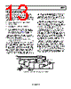
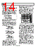
15 / 32 page  AD604 Rev. D | Page 15 of 32 The larger portion of the input referred voltage noise is coming from the amplifier with 0.63 nV/√Hz. The current noise is independent of gain and depends only on the bias current in the input stage of the preamplifier, which is 3 pA/√Hz. The preamplifier can drive 40 Ω (the nominal feedback resistors) and the following 175 Ω ladder load of the DSX with low distortion. For example, at 10 MHz and 1 V at the output, the preamplifier has less than −45 dB of second and third harmonic distortion when driven from a low (25 Ω) source resistance. In applications that require more than 48 dB of gain range, two AD604 channels can be cascaded. Because the preamplifier has a limited input signal range, consumes over half (120 mW) of the total power (220 mW), and its ultralow noise is not necessary after the first AD604 channel, a shutdown mechanism that disables only the preamplifier is provided. To shut down the preamplifier, connect the COM1 pin and/or COM2 pin to the positive supply; the DSX is unaffected. For additional details, refer to the Applications Information section. 12 11 10 9 8 1 2 3 4 7 6 5 13 16 15 14 24 23 22 21 20 19 18 17 AD604 –DSX1 +DSX1 PAI1 FBK1 PAO1 COM1 COM2 PAI2 FBK2 PAO2 +DSX2 –DSX2 VGN1 VREF VPOS GND1 OUT1 VNEG VNEG VPOS GND2 OUT2 VOCM VGN2 Figure 40. Shutdown of Preamplifiers Only DIFFERENTIAL LADDER (ATTENUATOR) The attenuator before the fixed gain amplifier of the DSX is realized by a differential 7-stage R-1.5R resistive ladder network with an untrimmed input resistance of 175 Ω single-ended or 350 Ω differential. The signal applied at the input of the ladder network is attenuated by 6.908 dB per tap; thus, the attenuation at the first tap is 0 dB, at the second, 13.816 dB, and so on, all the way to the last tap where the attenuation is 48.356 dB (see Figure 41). A unique circuit technique is used to interpolate continuously between the tap points, thereby providing continuous attenuation from 0 dB to −48.36 dB. The ladder network, together with the interpolation mechanism, can be considered a voltage-controlled potentiometer. Because the DSX circuit uses a single voltage power supply, the input biasing is provided by the VOCM buffer driving the MID node (see Figure 41). Without internal biasing, the user would have to dc bias the inputs externally. If not done carefully, the biasing network can introduce additional noise and offsets. By providing internal biasing, the user is relieved of this task and only needs to ac couple the signal into the DSX. Note that the input to the DSX is still fully differential if driven differentially, that is, Pin +DSX and Pin −DSX see the same signal but with opposite polarity (see the Ultralow Noise, Differential Input- Differential Output VGA section). What changes is the load seen by the driver; it is 175 Ω when each input is driven single-ended but 350 Ω when driven differentially. This is easily explained by thinking of the ladder network as two 175 Ω resistors connected back-to-back with the middle node, MID, being biased by the VOCM buffer. A differential signal applied between the +DSX and −DSX nodes results in zero current into the MID node, but a single-ended signal applied to either input, +DSX or −DSX, while the other input is ac grounded causes the current delivered by the source to flow into the VOCM buffer via the MID node. The ladder resistor value of 175 Ω provides the optimum balance between the load driving capability of the preamplifier and the noise contribution of the resistors. An advantage of the X-AMP architecture is that the output referred noise is constant vs. gain over most of the gain range. Figure 41 shows that the tap resistance is equal for all taps after only a few taps away from the inputs. The resistance seen looking into each tap is 54.4 Ω, which makes 0.95 nV/√Hz of Johnson noise spectral density. Because there are two attenuators, the overall noise contribution of the ladder network is √2 times 0.95 nV/√Hz or 1.34 nV/√Hz, a large fraction of the total DSX noise. The balance of the DSX circuit components contribute another 1.2 nV/√Hz, which together with the attenuator produces 1.8 nV/√Hz of total DSX input referred noise. R –6.908dB R 1.5R RR –13.82dB –20.72dB –27.63dB –34.54dB –41.45dB –48.36dB +DSX MID –DSX NOTES 1. R = 96Ω 2. 1.5R = 144Ω R R R R R R R R R R 1.5R 1.5R 1.5R 1.5R 1.5R 1.5R 1.5R 1.5R 1.5R 1.5R 1.5R 1.5R 1.5R 175Ω 175Ω Figure 41. R-1.5R Dual Ladder Network |
|
链接网址 |
| ALLDATASHEET是否为您带来帮助? [ DONATE ] |
关于 Alldatasheet | 广告服务 | 联系我们 | 隐私政策 | 数据表链接 | 链接交换 | 制造商名单 All Rights Reserved©Alldatasheet.com |
| Russian : Alldatasheetru.com | Korean : Alldatasheet.co.kr | Spanish : Alldatasheet.es | French : Alldatasheet.fr | Italian : Alldatasheetit.com Portuguese : Alldatasheetpt.com | Polish : Alldatasheet.pl | Vietnamese : Alldatasheet.vn Indian : Alldatasheet.in | Mexican : Alldatasheet.com.mx | British : Alldatasheet.co.uk | New Zealand : Alldatasheet.co.nz |
|
Family Site : ic2ic.com |
icmetro.com |
 Chinese ▼
 English
 Chinese
 German
 Japanese
 Russian
 Korean
 Spanish
 French
 Italian
 Portuguese
 Polish
 Vietnamese
 Indian
 Mexican
 British
 New Zealand