|
数据搜索系统,热门电子元器件搜索 |
|
|
数据搜索系统,热门电子元器件搜索 |
|
AD604ARSZ-R7 数据表(PDF) 19 Page - Analog Devices |
|
|
|||||||||||||||||||||||||||||
AD604ARSZ-R7 数据表(HTML) 19 Page - Analog Devices |
|
|
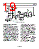
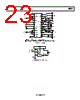
19 / 32 page  AD604 Rev. D | Page 19 of 32 VG 13 16 15 14 19 18 17 24 23 22 21 20 12 11 10 9 8 1 2 3 4 7 6 5 AD604 –5V +5V VREF RF OUT –5V +5V 8 7 6 5 1 2 3 4 AD711 NC OUT AD835 +5V –5V –5V +5V 2 VSET (<0V) –DSX1 +DSX1 PAI1 FBK1 PAO1 COM1 COM2 PAI2 FBK2 PAO2 +DSX2 –DSX2 VGN1 VREF VPOS GND1 OUT1 VNEG VNEG VPOS GND2 OUT2 VOCM VGN2 FB FB +5V –5V ALL SUPPLY PINS ARE DECOUPLED AS SHOWN. 1V OFFS NULL C1 0.1µF C2 0.1µF VIN (MAX 800mV p-p) R1 49.9Ω C3 0.1µF C4 0.1µF C12 0.1µF C13 0.1µF C7 0.1µF C6 0.56µF R2 453Ω R3 1kΩ C7 0.33µF V1 = VIN ×G R4 2kΩ C8 0.33µF 87 6 5 1 234 C9 0.33µF R5 2kΩ R6 2kΩ –(A)2 IF V1 = A × cos (wt) Y1 Y2 VN Z X1 X2 VP W –(V1)2 LOW- PASS FILTER R7 1kΩ C10 1µF C11 1µF R8 2kΩ +VS –VS OFFS NULL Figure 44. AGC Amplifier with 82 dB of Gain Range AN ULTRALOW NOISE AGC AMPLIFIER WITH 82 dB TO 96 dB GAIN RANGE Figure 44 shows an implementation of an AGC amplifier with 82 dB of gain range using a single AD604. The signal is applied to connector VIN, and because the signal source is 50 Ω, a terminating resistor (R1) of 49.9 Ω is added. The signal is then amplified by 14 dB (Pin FBK1 shorted to PAO1) through the Channel 1 preamplifier and is further processed by the Channel 1 DSX. Next, the signal is applied directly to the Channel 2 DSX. The second preamplifier is powered down by connecting its COM2 pin to the positive supply as explained in the Preamplifier section. C1 and C2 level shift the signal from the preamplifier into the first DSX and at the same time eliminate any offset contribution of the preamplifier. C3 and C4 have the same offset cancellation purpose for the second DSX. Each set of capacitors, combined with the 175 Ω input resistance of the corresponding DSX, provides a high-pass filter with a −3 dB corner frequency of about 9.1 kHz. VOCM is decoupled to ground by a 0.1 μF capacitor, while VREF can be externally provided; in this application, the gain scale is set to 20 dB/V by applying 2.500 V. Because each of the DSX amplifiers operates from a single 5 V supply, the output is ac-coupled via C6 and C7. The output signal can be monitored at the connector labeled RF OUT. Figure 45 and Figure 46 show the gain range and gain error for the AD604 connected as shown. The gain range is −14 dB to +82 dB; the useful range is 0 dB to +82 dB if the RF output amplitude is controlled to ±400 mV (+2 dBm). The main limitation on the lower end of the signal range is the input capability of the preamplifier. This limitation can be overcome by adding an attenuator in front of the preamplifier, but that would defeat the advantage of the ultralow noise preamplifier. It should be noted that the second preamplifier is not used because its ultralow noise and the associated high power consumption are overkill after the first DSX stage. It is disabled in this application by connecting the COM2 pin to the positive supply. Nevertheless, the second preamplifier can be used, if so desired, and the useful gain range increases by 14 dB to encompass 0 dB to 96 dB of gain. For the same +2 dBm output, this allows signals as small as −94 dBm to be measured. To achieve the highest gains, the input signal must be band- limited to reduce the noise; this is especially true if the second preamplifier is used. If the maximum signal at OUT2 of the AD604 is limited to ±400 mV (+2 dBm), the input signal level at the AGC threshold is +25 μV rms (−79 dBm). The circuit as shown in Figure 44 has about 40 MHz of noise bandwidth; the 0.8 nV/√Hz of input referred voltage noise spectral density of the AD604 results in an rms noise of 5.05 μV in the 40 MHz bandwidth. |
|
链接网址 |
| ALLDATASHEET是否为您带来帮助? [ DONATE ] |
关于 Alldatasheet | 广告服务 | 联系我们 | 隐私政策 | 数据表链接 | 链接交换 | 制造商名单 All Rights Reserved©Alldatasheet.com |
| Russian : Alldatasheetru.com | Korean : Alldatasheet.co.kr | Spanish : Alldatasheet.es | French : Alldatasheet.fr | Italian : Alldatasheetit.com Portuguese : Alldatasheetpt.com | Polish : Alldatasheet.pl | Vietnamese : Alldatasheet.vn Indian : Alldatasheet.in | Mexican : Alldatasheet.com.mx | British : Alldatasheet.co.uk | New Zealand : Alldatasheet.co.nz |
|
Family Site : ic2ic.com |
icmetro.com |
 Chinese ▼
 English
 Chinese
 German
 Japanese
 Russian
 Korean
 Spanish
 French
 Italian
 Portuguese
 Polish
 Vietnamese
 Indian
 Mexican
 British
 New Zealand