|
数据搜索系统,热门电子元器件搜索 |
|
|
数据搜索系统,热门电子元器件搜索 |
|
AD604ARSZ-R7 数据表(PDF) 21 Page - Analog Devices |
|
|
|||||||||||||||||||||||||||||
AD604ARSZ-R7 数据表(HTML) 21 Page - Analog Devices |
|
|
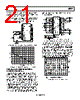
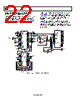
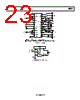
21 / 32 page  AD604 Rev. D | Page 21 of 32 At 1 MHz, the attenuation is about −0.2 dB, increasing to −6 dB at 10 MHz and −28 dB at 100 MHz. Signals less than approximately 1 MHz are not significantly affected. Figure 49 shows the control voltage vs. the input power at 1 MHz to the circuit in Figure 48; note that the AGC threshold is at −95 dBm. The output signal level is set to 800 mV p-p by applying −80 mV to the VSET connector. 12 11 10 9 8 1 2 3 4 7 6 5 13 16 15 14 24 23 22 21 20 19 18 17 AD604 FB –DSX1 +DSX1 PAI1 FBK1 PAO1 COM1 COM2 PAI2 FBK2 PAO2 +DSX2 –DSX2 VGN1 VREF VPOS GND1 OUT1 VNEG VNEG VPOS GND2 OUT2 VOCM VGN2 FAIR-RITE #2643000301 C5 0.1µF R2 499Ω C6 560pF C3 0.1µF Figure 48. Modifications of AGC Amplifier to Create 96 dB of Gain Range 4.5 4.0 0 3.5 3.0 1.0 2.5 2.0 1.5 1MHz 0.5 PIN (dBm) –100 –90 –80 –70 –60 –50 –40 –30 –20 –10 0 10 Figure 49. Control Voltage vs. Input Power of Circuit in Figure 48 ULTRALOW NOISE, DIFFERENTIAL INPUT- DIFFERENTIAL OUTPUT VGA Figure 50 shows how to use both preamplifiers and DSXs to create a high impedance, differential input-differential output VGA. This application takes advantage of the differential inputs to the DSXs. Note that the input is not truly differential in the sense that the common-mode voltage needs to be at ground to achieve maximum input signal swing. This has largely to do with the limited output swing capability of the output drivers of the preamplifiers; they clip around ±2.2 V due to having to drive an effective load of about 30 Ω. If a different input common-mode voltage needs to be accommodated, ac coupling (as was done in Figure 48) is recommended. The differential gain range of this circuit runs from 6 dB to 54 dB, which is 6 dB higher than each individual channel of the AD604 because the DSX inputs now see twice the signal amplitude compared to when they are driven single-ended. 13 16 15 14 19 18 17 24 23 22 21 20 12 11 10 9 8 1 2 3 4 7 6 5 AD604 FB FB +5V –5V ALL SUPPLY PINS ARE DECOUPLED AS SHOWN. +5V –5V –5V +5V VIN+ VIN– VG VREF VOUT+ VOUT– –DSX1 +DSX1 PAI1 FBK1 PAO1 COM1 COM2 PAI2 FBK2 PAO2 +DSX2 –DSX2 VGN1 VREF VPOS GND1 OUT1 VNEG VNEG VPOS GND2 OUT2 VOCM VGN2 C13 0.1µF C12 0.1µF C1 0.1µF C2 0.1µF C4 0.1µF C3 0.1µF C5 0.1µF C7 0.1µF R1 453Ω R2 453Ω C6 0.1µF Figure 50. Ultralow Noise, Differential Input-Differential Output VGA Figure 51 displays the output signals VOUT+ and VOUT− after a −20 dB attenuator formed between the 453 Ω resistors shown in Figure 50 and the 50 Ω loads presented by the oscilloscope plug-in. R1 and R2 are inserted to ensure a nominal load of 500 Ω at each output. The differential gain of the circuit is set to 20 dB by applying a control voltage, VGN, of 1 V; the gain scaling is 20 dB/V for a VREF of 2.500 V; the input frequency is 10 MHz and the differential input amplitude is 100 mV p-p. The resulting differential output amplitude is 1 V p-p as can be seen on the scope photo when reading the vertical scale as 200 mV/div. 10 0% 100 90 20ns 20mV 20mV NOTES 1. THE OUTPUT AFTER 10× ATTENUATER FORMED BY 453Ω TOGETHER WITH 50Ω OF 7A24 PLUG-IN. –500mV ACTUAL VOUT +500mV Figure 51. Output of VGA in Figure 50 for VGN = 1 V |
|
链接网址 |
| ALLDATASHEET是否为您带来帮助? [ DONATE ] |
关于 Alldatasheet | 广告服务 | 联系我们 | 隐私政策 | 数据表链接 | 链接交换 | 制造商名单 All Rights Reserved©Alldatasheet.com |
| Russian : Alldatasheetru.com | Korean : Alldatasheet.co.kr | Spanish : Alldatasheet.es | French : Alldatasheet.fr | Italian : Alldatasheetit.com Portuguese : Alldatasheetpt.com | Polish : Alldatasheet.pl | Vietnamese : Alldatasheet.vn Indian : Alldatasheet.in | Mexican : Alldatasheet.com.mx | British : Alldatasheet.co.uk | New Zealand : Alldatasheet.co.nz |
|
Family Site : ic2ic.com |
icmetro.com |
 Chinese ▼
 English
 Chinese
 German
 Japanese
 Russian
 Korean
 Spanish
 French
 Italian
 Portuguese
 Polish
 Vietnamese
 Indian
 Mexican
 British
 New Zealand