|
数据搜索系统,热门电子元器件搜索 |
|
|
数据搜索系统,热门电子元器件搜索 |
|
M24LR04E-R 数据表(PDF) 14 Page - STMicroelectronics |
|
|
|||||||||||||||||||||||||||||
M24LR04E-R 数据表(HTML) 14 Page - STMicroelectronics |
|
|
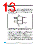
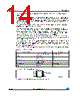
14 / 142 page  Description M24LR04E-R 14/142 Doc ID 022208 Rev 5 using the 1/256 pulse coding mode or a data rate of 26 Kbit/s using the 1/4 pulse coding mode. Outgoing data are generated by the M24LR04E-R load variation using Manchester coding with one or two subcarrier frequencies at 423 kHz and 484 kHz. Data are transferred from the M24LR04E-R at 6.6 Kbit/s in low data rate mode and 26 Kbit/s high data rate mode. The M24LR04E-R supports the 53 Kbit/s fast mode in high data rate mode using one subcarrier frequency at 423 kHz. The M24LR04E-R follows the ISO 15693 and ISO 18000-3 mode 1 recommendation for radio-frequency power and signal interface. The M24LR04E-R provides an Energy harvesting mode on the analog output pin Vout. When the Energy harvesting mode is activated, the M24LR04E-R can output the excess energy coming from the RF field on the Vout analog pin. In case the RF field strength is insufficient or when Energy harvesting mode is disabled, the analog output pin Vout goes into high-Z state and Energy harvesting mode is automatically stopped. The M24LR04E-R features a user configurable digital out pin RF WIP/BUSY that can be used to drive a micro controller interrupt input pin (available only when the M24LR04E-R is correctly powered on the Vcc pin). When configured in the RF write in progress mode (RF WIP mode), the RF WIP/BUSY pin is driven low for the entire duration of the RF internal write operation. When configured in the RF busy mode (RF BUSY mode), the RF WIP/BUSY pin is driven low for the entire duration of the RF command progress. The RF WIP/BUSY pin is an open drain output and must be connected to a pull-up resistor. Figure 2. 8-pin package connections 1. See Section 30 for package dimensions, and how to identify pin-1. Table 1. Signal names Signal name Function Direction Vout Energy harvesting Output Analog output SDA Serial Data I/O SCL Serial Clock Input AC0, AC1 Antenna coils I/O VCC Supply voltage RF WIP/BUSY Digital signal Digital output VSS Ground SDA VSS SCL RF WIP/BUSY AC0 Vout VCC MS19742V1 1 2 3 4 8 7 6 5 AC1 |
|
链接网址 |
| ALLDATASHEET是否为您带来帮助? [ DONATE ] |
关于 Alldatasheet | 广告服务 | 联系我们 | 隐私政策 | 数据表链接 | 链接交换 | 制造商名单 All Rights Reserved©Alldatasheet.com |
| Russian : Alldatasheetru.com | Korean : Alldatasheet.co.kr | Spanish : Alldatasheet.es | French : Alldatasheet.fr | Italian : Alldatasheetit.com Portuguese : Alldatasheetpt.com | Polish : Alldatasheet.pl | Vietnamese : Alldatasheet.vn Indian : Alldatasheet.in | Mexican : Alldatasheet.com.mx | British : Alldatasheet.co.uk | New Zealand : Alldatasheet.co.nz |
|
Family Site : ic2ic.com |
icmetro.com |
 Chinese ▼
 English
 Chinese
 German
 Japanese
 Russian
 Korean
 Spanish
 French
 Italian
 Portuguese
 Polish
 Vietnamese
 Indian
 Mexican
 British
 New Zealand