|
数据搜索系统,热门电子元器件搜索 |
|
|
数据搜索系统,热门电子元器件搜索 |
|
M24LR04E-R 数据表(PDF) 27 Page - STMicroelectronics |
|
|
|||||||||||||||||||||||||||||
M24LR04E-R 数据表(HTML) 27 Page - STMicroelectronics |
|
|
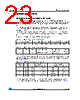
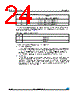
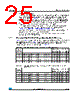
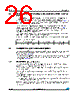
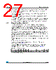
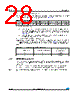
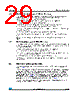
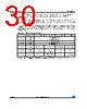
27 / 142 page  M24LR04E-R System memory area Doc ID 022208 Rev 5 27/142 When tied to 0, the RF WIP/BUSY signal returns to High-Z state if the RF field is cut-off. During execution of I²C commands, the RF WIP/BUSY pin remains in high-Z state. ● RF Write in progress When bit 3 of the Configuration byte is set to 1, the RF WIP/BUSY pin is configured in RF Write in progress mode. The purpose of this mode is to indicate to the I²C bus master that some data have been changed in RF mode. In this mode, the RF WIP/BUSY pin is tied to 0 for the duration of an internal write operation (i.e. between the end of a valid RF write command and the beginning of the RF answer). During execution of I²C write operations, the RF WIP/BUSY pin remains in high-Z state. 4.3.2 Energy harvesting configuration The M24LR04E-R features an Energy harvesting mode on the Vout analog output. The general purpose of the Energy harvesting mode is to deliver a part of the non- necessary RF power received by the M24LR04E-R on the AC0-AC1 RF input in order to supply an external device. The current consumption on the analog voltage output Vout is limited to ensure that the M24LR04E-R is correctly supplied during the powering of the external device. When the Energy harvesting mode is enabled and the power delivered on the AC0-AC1 RF input exceeds the minimum required PAC0-AC1_min, the M24LR04E-R is able to deliver a limited and unregulated voltage on the Vout pin, assuming the current consumption on the Vout does not exceed the Isink_max maximum value. If one of the condition above is not met, the analog voltage output pin Vout is set in High-Z state. For robust applications using the Energy harvesting mode, four current fan-out levels can be chosen. ● Vout sink current configuration The sink current level is chosen by programming EH_cfg1 and EH_cfg0 into the Configuration byte (see Table 14). The minimum power level required on AC0-AC1 RF input PAC0-AC1_min, the delivered voltage Vout, as well as the maximum current consumption Isink_max on the Vout pin corresponding to the <EH_cfg1,EH_cfg0> bit values are described in Table 125. Table 14. Configuration byte I2C byte address Bit 7 Bit 6 Bit 5 Bit 4 Bit 3 Bit 2 BIT 1 BIT 0 E2=1 2320 X(1) 1. Bit 7 to Bit 4 are don’t care bits. X(1) X(1) X(1) RF WIP/BUSY EH_mode EH_cfg1 EH_cfg0 |
|
链接网址 |
| ALLDATASHEET是否为您带来帮助? [ DONATE ] |
关于 Alldatasheet | 广告服务 | 联系我们 | 隐私政策 | 数据表链接 | 链接交换 | 制造商名单 All Rights Reserved©Alldatasheet.com |
| Russian : Alldatasheetru.com | Korean : Alldatasheet.co.kr | Spanish : Alldatasheet.es | French : Alldatasheet.fr | Italian : Alldatasheetit.com Portuguese : Alldatasheetpt.com | Polish : Alldatasheet.pl | Vietnamese : Alldatasheet.vn Indian : Alldatasheet.in | Mexican : Alldatasheet.com.mx | British : Alldatasheet.co.uk | New Zealand : Alldatasheet.co.nz |
|
Family Site : ic2ic.com |
icmetro.com |
 Chinese ▼
 English
 Chinese
 German
 Japanese
 Russian
 Korean
 Spanish
 French
 Italian
 Portuguese
 Polish
 Vietnamese
 Indian
 Mexican
 British
 New Zealand