|
数据搜索系统,热门电子元器件搜索 |
|
|
数据搜索系统,热门电子元器件搜索 |
|
M24LR04E-R 数据表(PDF) 26 Page - STMicroelectronics |
|
|
|||||||||||||||||||||||||||||
M24LR04E-R 数据表(HTML) 26 Page - STMicroelectronics |
|
|
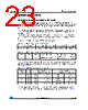
26 / 142 page  System memory area M24LR04E-R 26/142 Doc ID 022208 Rev 5 4.2 M24LR04E-R block security in I²C mode (I2C_Write_Lock bit area) In the I2C mode only, it is possible to protect individual sectors against Write operations. This feature is controlled by the I2C_Write_Lock bits stored in the 2 bytes of the I2C_Write_Lock bit area. I2C_Write_Lock bit area starts from location 2048 (see Table 13). To access the I2C_Write_Lock bit area, the device select code used for any I2C command must have the E2 Chip Enable address at 1. Using these 16 bits, it is possible to write-protect all the 4 sectors of the M24LR04E-R memory. Each bit controls the I2C write access to a specific sector as shown in Table 13. It is always possible to unprotect a sector in the I2C mode. When an I2C_Write_Lock bit is reset to 0, the corresponding sector is unprotected. When the bit is set to 1, the corresponding sector is write-protected. In I2C mode, read access to the I2C_Write_Lock bit area is always allowed. Write access depends on the correct presentation of the I2C password. On delivery, the default value of the two bytes of the I2C_Write_Lock bit area is reset to 00h. m 4.3 Configuration byte and Control register The M24LR04E-R offers an 8-bit non-volatile Configuration byte located at I²C location 2320 of the system area used to store the RF WIP/BUSY pin and the energy harvesting configuration (see Table 14). The M24LR04E-R also offers an 8-bit volatile Control register located at I²C location 2336 of the system area used to store the energy harvesting enable bit as well as a FIELD_ON bit indicator (see Table 15). 4.3.1 RF WIP/BUSY pin configuration The M24LR04E-R features a configurable open drain output RF WIP/BUSY pin used to provide RF activity information to an external device. The RF WIP/BUSY pin functionality depends on the value of bit 3 of the Configuration byte. ● RF busy mode When bit 3 of the Configuration byte is set to 0, the RF WIP/BUSY pin is configured in RF busy mode. The purpose of this mode is to indicate to the I²C bus master whether the M24LR04E-R is busy in RF mode or not. In this mode, the RF WIP/BUSY pin is tied to 0 from the RF command Start Of Frame (SOF) until the end of the command execution. If a bad RF command is received, the RF WIP/BUSY pin is tied to 0 from the RF command SOF until the reception of the RF command CRC. Otherwise, the RF WIP/BUSY pin is in high-Z state. Table 13. I2C_Write_Lock bit I2C byte address Bits [4:15] Bits [3:0] E2 = 1 2048 Don’t care sectors 0-3 |
|
链接网址 |
| ALLDATASHEET是否为您带来帮助? [ DONATE ] |
关于 Alldatasheet | 广告服务 | 联系我们 | 隐私政策 | 数据表链接 | 链接交换 | 制造商名单 All Rights Reserved©Alldatasheet.com |
| Russian : Alldatasheetru.com | Korean : Alldatasheet.co.kr | Spanish : Alldatasheet.es | French : Alldatasheet.fr | Italian : Alldatasheetit.com Portuguese : Alldatasheetpt.com | Polish : Alldatasheet.pl | Vietnamese : Alldatasheet.vn Indian : Alldatasheet.in | Mexican : Alldatasheet.com.mx | British : Alldatasheet.co.uk | New Zealand : Alldatasheet.co.nz |
|
Family Site : ic2ic.com |
icmetro.com |
 Chinese ▼
 English
 Chinese
 German
 Japanese
 Russian
 Korean
 Spanish
 French
 Italian
 Portuguese
 Polish
 Vietnamese
 Indian
 Mexican
 British
 New Zealand