|
数据搜索系统,热门电子元器件搜索 |
|
|
数据搜索系统,热门电子元器件搜索 |
|
AD7687BCPZ-R2 数据表(PDF) 20 Page - Analog Devices |
|
|
|||||||||||||||||||||||||||||
AD7687BCPZ-R2 数据表(HTML) 20 Page - Analog Devices |
|
|
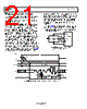
20 / 27 page  Data Sheet AD7687 Rev. E | Page 19 of 26 CS MODE, 3-WIRE WITHOUT BUSY INDICATOR This mode is usually used when a single AD7687 is connected to an SPI-compatible digital host. Figure 34 shows the connection diagram and Figure 35 gives the corresponding timing. With SDI tied to VIO, a rising edge on CNV initiates a conversion, selects the CS mode, and forces SDO to high impedance. Once a conversion is initiated, it continues to completion irrespective of the state of CNV. For instance, it can be useful to bring CNV low to select other SPI devices, such as analog multiplexers, but CNV must be returned high before the minimum conversion time and held high until the maximum conversion time to avoid the generation of the BUSY signal indicator (see tCONV in Table 5). When the conversion is complete, the AD7687 enters the acquisition phase and powers down. When CNV goes low, the MSB is output onto SDO. The remaining data bits are then clocked by subsequent SCK falling edges. The data is valid on both SCK edges. Although the rising edge can capture the data, a digital host using the SCK falling edge allows a faster reading rate (provided it has an acceptable hold time). After the 16th SCK falling edge, or when CNV goes high, whichever is earlier, SDO returns to high impedance. CNV SCK SDO SDI DATA IN CLK CONVERT VIO DIGITAL HOST AD7687 Figure 34. CS Mode, 3-Wire Without BUSY Indicator Connection Diagram (SDI High) SDO D15 D14 D13 D1 D0 tDIS SCK 1 2 3 14 15 16 tSCK tSCKL tSCKH tHSDO tDSDO CNV CONVERSION ACQUISITION tCONV tCYC ACQUISITION SDI = 1 tCNVH tACQ tEN Figure 35. CS Mode, 3-Wire Without BUSY Indicator Serial Interface Timing (SDI High) |
|
|
链接网址 |
| ALLDATASHEET是否为您带来帮助? [ DONATE ] |
关于 Alldatasheet | 广告服务 | 联系我们 | 隐私政策 | 数据表链接 | 链接交换 | 制造商名单 All Rights Reserved©Alldatasheet.com |
| Russian : Alldatasheetru.com | Korean : Alldatasheet.co.kr | Spanish : Alldatasheet.es | French : Alldatasheet.fr | Italian : Alldatasheetit.com Portuguese : Alldatasheetpt.com | Polish : Alldatasheet.pl | Vietnamese : Alldatasheet.vn Indian : Alldatasheet.in | Mexican : Alldatasheet.com.mx | British : Alldatasheet.co.uk | New Zealand : Alldatasheet.co.nz |
|
Family Site : ic2ic.com |
icmetro.com |
 Chinese ▼
 English
 Chinese
 German
 Japanese
 Russian
 Korean
 Spanish
 French
 Italian
 Portuguese
 Polish
 Vietnamese
 Indian
 Mexican
 British
 New Zealand