|
数据搜索系统,热门电子元器件搜索 |
|
|
数据搜索系统,热门电子元器件搜索 |
|
EM62100AGH 数据表(PDF) 15 Page - ELAN Microelectronics Corp |
|
|
|||||||||||||||||||||||||||||
EM62100AGH 数据表(HTML) 15 Page - ELAN Microelectronics Corp |
|
|
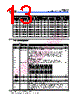
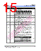
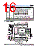
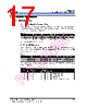
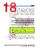
15 / 60 page  EM62100 65 COM/132 SEG STN LCD Driver Product Specification (V1.1) 09.13.2005 •••• 9 (This specification is subject to change without further notice) Pin Name I/O Function No.ofPins M/S = “H”: Master operation M/S = “L”: Slave operation The following is true depending on the M/S and CKS status: M/S CKS Oscillator Circuit PowerSupply Circuit CK M FLM DOFB H Enable Enable O O O O H L Disable Enable I O O O L - Disable Disable I I O I 1 M/S I O: Output, I: Input CK I/O Display clock input terminal When the EM62100 chips are used in master/slave mode, the various CK terminals must be connected. 1 M I/O Liquid crystal alternating current signal I/O terminal. M/S = “H”: Output, M/S = “L”: Input When the EM62100 Series chip is used in master/slave mode, the various M terminals must be connected. 1 DOFB I/O LCD blanking control terminal M/S = “H”: Output, M/S = “L”: Input When the EM62100 chip is used in master/slave mode, the various DOFB terminals must be connected. 1 FLM O Output terminal for the static drive This terminal is only enabled when the static indicator display is ON during master mode operation, and is used in connection with the M terminal. 1 IRS I This terminal selects the resistors for the V0 voltage level adjustment. IRS = “H”: Use the internal resistors IRS = “L”: Do not use the internal resistors. The V0 voltage level is regulated by an external resistive voltage divider attached to the VREF terminal. This pin is enabled only when master mode operation is selected. It is fixed to either “H” or “L” when slave mode operation is selected. 1 HPMB I Power control terminal for the power supply circuit for liquid crystal drive. HPMB = “H”: Normal mode, HPMB = “L”: High power mode This pin is enabled only when master mode operation is selected. It is fixed to either “H” or “L” when slave mode operation is selected. 1 Liquid crystal segment drive outputs. Through a combination of the contents of the display RAM and with the M signal, a single level is selected from V0, V2, V3, and VSS. RAM DATA M Output Voltage Normal Display Reverse Display H H V0 V2 H L VSS V3 L H V2 V0 L L V3 VSS Power Save & Display OFF -- VSS SEG0 To SEG131 O 132 |
|
链接网址 |
| ALLDATASHEET是否为您带来帮助? [ DONATE ] |
关于 Alldatasheet | 广告服务 | 联系我们 | 隐私政策 | 数据表链接 | 链接交换 | 制造商名单 All Rights Reserved©Alldatasheet.com |
| Russian : Alldatasheetru.com | Korean : Alldatasheet.co.kr | Spanish : Alldatasheet.es | French : Alldatasheet.fr | Italian : Alldatasheetit.com Portuguese : Alldatasheetpt.com | Polish : Alldatasheet.pl | Vietnamese : Alldatasheet.vn Indian : Alldatasheet.in | Mexican : Alldatasheet.com.mx | British : Alldatasheet.co.uk | New Zealand : Alldatasheet.co.nz |
|
Family Site : ic2ic.com |
icmetro.com |
 Chinese ▼
 English
 Chinese
 German
 Japanese
 Russian
 Korean
 Spanish
 French
 Italian
 Portuguese
 Polish
 Vietnamese
 Indian
 Mexican
 British
 New Zealand