|
数据搜索系统,热门电子元器件搜索 |
|
|
数据搜索系统,热门电子元器件搜索 |
|
STDRIVEG611QTR 数据表(PDF) 6 Page - STMicroelectronics |
|
|
|||||||||||||||||||||||||||||
STDRIVEG611QTR 数据表(HTML) 6 Page - STMicroelectronics |
|
|
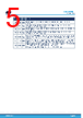
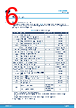
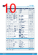
6 / 33 page  4 Device ratings 4.1 Absolute maximum ratings Stresses above the absolute maximum ratings listed in Table 2 may cause permanent damage to the device. Exposure to maximum rating conditions for extended periods may affect device reliability. All voltages referred to ground pins unless otherwise specified. Table 2. Absolute maximum ratings Symbol Parameter Test condition Value Unit VCC Logic supply voltage -0.3 to 21 V PGND Low-side driver ground vs. logic ground VCC = 14 V -7 to 7 V VVCC-PGND Logic supply vs. low-side driver ground -0.3 to 21 V VVCCL_max Regulated low-side driver supply vs. logic ground -0.3 to 21 V VLS Regulated low-side driver supply voltage (1) (2) -0.3 to 21 V ILS_OUT Low-side regulator maximum current (1) (2) Self-limited A VVCC-VCCL_max Maximum low-side dropout voltage -0.3 to self-regulated V VOUTL_max Low-side output to PGND voltage DC values -0.3 to VCCL+0.3 V VRONL_max Low-side turn-on resistor pin max. voltage VOUTL-0.3 to VCCL+0.3 V VBOOT BOOT pin voltage referred to GND -0.3 to 621 V VBO High-side regulator input voltage (1) -0.3 to 21 V VHS Regulated high-side driver supply voltage (1) (2) -0.3 to 21 V IHS_OUT High-side regulator maximum current (1) (2) Self-limited A VBOOT-VCCH_max Maximum high-side dropout voltage -0.3 to self-regulated V VOUTH_max High-side output to OUT voltage DC values -0.3 to VCCH+0.3 V VRONH_max High-side turn-on resistor pin max. voltage VOUTH-0.3 to VCCH+0.3 V dVOUT/dt_max Maximum OUT voltage slew rate (3) 200 V/ns CIN Comparator input voltage -0.3 to 21 V Vin_max Logic inputs voltage range (LIN, HIN, SD/OD, STBY, FLT) -0.3 to 21 V IFLT_max Maximum FLT pin current (DC inward) VCC = 7 V 10 mA IOD_max Maximum SD/OD pin current (DC inward) VCC = 12 V 10 mA TJ Junction temperature -40 to 150 °C Tstg Storage temperature -55 to 150 °C ESD HBM (Human Body Model) ANSI/ESDA/JEDEC JS-001-2017 2 (4) kV CDM (Charged Device Model) ANSI/ESDA/JEDEC JS-002-2018 1 kV 1. VLS = VVCCL-PGND, VHS = VVCCH-OUT, VBO = VBOOT-OUT. 2. The internal low-side and high-side voltage regulators are not intended to be connected to external load nor voltage sources. 3. Range estimated by characterization on a limited number of samples, not tested in production. 4. High voltage pin 18 vs. GND has 1500 V rating STDRIVEG611 Device ratings DS14457 - Rev 2 page 6/33 |
|
链接网址 |
| ALLDATASHEET是否为您带来帮助? [ DONATE ] |
关于 Alldatasheet | 广告服务 | 联系我们 | 隐私政策 | 数据表链接 | 链接交换 | 制造商名单 All Rights Reserved©Alldatasheet.com |
| Russian : Alldatasheetru.com | Korean : Alldatasheet.co.kr | Spanish : Alldatasheet.es | French : Alldatasheet.fr | Italian : Alldatasheetit.com Portuguese : Alldatasheetpt.com | Polish : Alldatasheet.pl | Vietnamese : Alldatasheet.vn Indian : Alldatasheet.in | Mexican : Alldatasheet.com.mx | British : Alldatasheet.co.uk | New Zealand : Alldatasheet.co.nz |
|
Family Site : ic2ic.com |
icmetro.com |
 Chinese ▼
 English
 Chinese
 German
 Japanese
 Russian
 Korean
 Spanish
 French
 Italian
 Portuguese
 Polish
 Vietnamese
 Indian
 Mexican
 British
 New Zealand