|
数据搜索系统,热门电子元器件搜索 |
|
|
数据搜索系统,热门电子元器件搜索 |
|
STDRIVEG611QTR 数据表(PDF) 4 Page - STMicroelectronics |
|
|
|||||||||||||||||||||||||||||
STDRIVEG611QTR 数据表(HTML) 4 Page - STMicroelectronics |
|
|
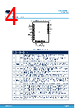
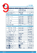
4 / 33 page  3 Pin description Figure 4. STDRIVEG611 pin connection RONH VCCH OUT OUTH BOOT HIN LIN FLT SD/OD CIN VCC STBY GND 2 3 4 5 1 7 6 8 9 10 11 12 13 14 15 17 16 18 Table 1. STDRIVEG611 pin list Pin N. Name Type Function 1 VCC Power Supply voltage of logic section. A small bypass capacitor (100 nF typ.) very close to the pin is required to get a clean bias voltage for the signal part of the IC. The large bulk capacitor that is normally used to supply the controller is sufficient to supply the STDRIVEG611 as well: if not present, a value larger than 2.2 µF is suggested. The input of the low-side driver regulator is internally connected to this pin. 2 STBY Input Standby mode activation pin. Setting this pin to GND, the IC enters a low consumption mode to facilitate the design of low consumption topologies. The internal pull-down resistor is there to avoid uncertain voltage application when IC is not biased. 3, 9 GND Power Ground pins. Common potential of the Logic section of the device. These pins have both an electrical and thermal purpose: tying these pins to a proper copper area effectively enhances power dissipation (typically required only on high frequency applications). 4 CIN Input Comparator input pin for SmartSD. In case of triggering, both GaN are immediately turned off and SD/OD is pulled low. Connect to GND if not used. 5 FLT Output Fault signaling pin. An open drain MOSFET is turned on to pull the FLT pin down when UVLO, standby, comparator, or overtemperature protection are active. Connect to GND if not used. 6 SD/OD Input/ Output Shutdown input (active low) / open drain output for comparator with smartSD. When this pin is pulled to GND, the IC immediately interrupts the switching activity defined by LIN and HIN. When CIN exceeds the threshold, SmartSD interrupts the switching activity and pulls low the SD/OD pin. Once the overcurrent ends, the open drain is released. The internal pull-down resistor is there to avoid uncertain voltage application when IC is not biased. 7 HIN Input High-side logic input pin. Driving pulses to control the high-side switch can be applied to this pin. A Schmitt trigger comparator, 20 V tolerant, buffers the input signal before driving level shifters. 8 LIN Input Low-side logic input pin. Driving pulses to control the low-side switch can be applied to this pin. A Schmitt trigger comparator, 20 V tolerant, buffers the input signal before driving level shifters. 10 VCCL Power Output of the linear regulator that supplies the output stage of the low-side driver. A ceramic capacitor equal or greater than 47 nF (X7R, 16 V) must be placed as close as possible between this pin and PGND. 11 RONL Output A resistor connected between this pin and VCCL sets the turn-on resistor source current of the low- side driver. Mounting the resistor as close as possible to the RONL pin optimizes the operation of the driver. STDRIVEG611 Pin description DS14457 - Rev 2 page 4/33 |
|
链接网址 |
| ALLDATASHEET是否为您带来帮助? [ DONATE ] |
关于 Alldatasheet | 广告服务 | 联系我们 | 隐私政策 | 数据表链接 | 链接交换 | 制造商名单 All Rights Reserved©Alldatasheet.com |
| Russian : Alldatasheetru.com | Korean : Alldatasheet.co.kr | Spanish : Alldatasheet.es | French : Alldatasheet.fr | Italian : Alldatasheetit.com Portuguese : Alldatasheetpt.com | Polish : Alldatasheet.pl | Vietnamese : Alldatasheet.vn Indian : Alldatasheet.in | Mexican : Alldatasheet.com.mx | British : Alldatasheet.co.uk | New Zealand : Alldatasheet.co.nz |
|
Family Site : ic2ic.com |
icmetro.com |
 Chinese ▼
 English
 Chinese
 German
 Japanese
 Russian
 Korean
 Spanish
 French
 Italian
 Portuguese
 Polish
 Vietnamese
 Indian
 Mexican
 British
 New Zealand