|
数据搜索系统,热门电子元器件搜索 |
|
|
数据搜索系统,热门电子元器件搜索 |
|
STDRIVEG611QTR 数据表(PDF) 15 Page - STMicroelectronics |
|
|
|||||||||||||||||||||||||||||
STDRIVEG611QTR 数据表(HTML) 15 Page - STMicroelectronics |
|
|
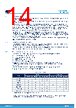
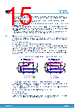
15 / 33 page  The front-end of logic inputs consists of a comparator having a fixed threshold and defined hysteresis to guarantee precise and robust level detection. The input pins can accept an input voltage up to 20 V independently from VCC voltage level. Propagation delays between LIN and HIN input pins to OUTL and OUTH are matched to obtain the best symmetry and minimum pulse width distortion. The minimum duration of the pulse that can be transferred from LIN and HIN to OUTL and OUTH is tINmin; shorter pulses may be blanked. The FLT open drain pin signals standby, UVLO (VCC and VCCL), overcurrent, and overtemperature status. An external pull-up resistor or source current is required to raise the FLT pin signal. The maximum pull-up voltage is 20 V, independent from VCC. When unused, this pin must be connected to GND. The STBY pin is intended to activate standby mode to reduce the IC consumption during long-lasting inactive times or between burst modes. The description of this mode is reported in Section 6.5. 6.3 Gate driving outputs and gate resistors The STDRIVEG611 has a gate driver output architecture enabling turn-on and turn-off impedance differentiation to tune dV/dt and dI/dt avoiding turn-off diode usage. Diode avoidance for turn-on/off differentiation has several benefits: • bill of material (BOM) reduction; • gate loop inductance minimization due to smaller geometrical gate loop; • more effective and faster turn-off with increased induced turn-on margin thanks to diode VF drop removal. Effective turn-off is crucial with GaN switches due to low VGSth and turn-off diode is typically not recommended especially with unipolar gate driving (no negative VGS while off). Similarly to STDRIVEG600 (classic separated output architecture), with the STDRIVEG611 (single gate output architecture) the gate turn-on/off currents can be tuned by external resistors, but those resistors are arranged in different way. Figure 11. Gate driver output and gate resistor tuning for differentiated turn-on/off Driver VCCx RONx OUTx PGND/OUT RON CVCCx GATE R STDRIVEG61x Driver PVCC/BOOT xON xOFF PGND/OUT CPVCC/ BOOT OFF R STDRIVEG600 ON R Gate charge path Gate discharge path Gate discharge path Gate charge path RSO RSI RSO RSI "CLASSIC" SEPARATED OUTPUTS SINGLE GATE OUTPUT Turn-off: RSI + RGATE Turn-on: RSO + RON + RGATE Turn-off: RSI + ROFF Turn-on: RSO + RON Turn-off path goes through RGATE, so the user shall increase RGATE to slow down turn-off speed. Increasing RGATE will slow down also turn-on speed since turn-on path goes through RGATE and RON. The user shall increase RON to further slowdown turn-on speed. Thus, turn-on impedance can be only equal or higher than turn-off, as typically found in all applications to avoid induced turn-on phenomenon. As rule-of-thumb when migrating from “classic” separated output architectures: • RGATE≈ ROFF(old) • RON≈ RON(old) - RGATE In power conversion applications, depending on gate charge, turn-off resistor (RGATE) is typically in the range of 1 to 5 Ω while turn-on resistance sum (RGATE + RON) is typically in the range of 5 to 300 Ω. STDRIVEG611 Device description DS14457 - Rev 2 page 15/33 |
|
链接网址 |
| ALLDATASHEET是否为您带来帮助? [ DONATE ] |
关于 Alldatasheet | 广告服务 | 联系我们 | 隐私政策 | 数据表链接 | 链接交换 | 制造商名单 All Rights Reserved©Alldatasheet.com |
| Russian : Alldatasheetru.com | Korean : Alldatasheet.co.kr | Spanish : Alldatasheet.es | French : Alldatasheet.fr | Italian : Alldatasheetit.com Portuguese : Alldatasheetpt.com | Polish : Alldatasheet.pl | Vietnamese : Alldatasheet.vn Indian : Alldatasheet.in | Mexican : Alldatasheet.com.mx | British : Alldatasheet.co.uk | New Zealand : Alldatasheet.co.nz |
|
Family Site : ic2ic.com |
icmetro.com |
 Chinese ▼
 English
 Chinese
 German
 Japanese
 Russian
 Korean
 Spanish
 French
 Italian
 Portuguese
 Polish
 Vietnamese
 Indian
 Mexican
 British
 New Zealand