|
数据搜索系统,热门电子元器件搜索 |
|
|
数据搜索系统,热门电子元器件搜索 |
|
STDRIVEG611QTR 数据表(PDF) 22 Page - STMicroelectronics |
|
|
|||||||||||||||||||||||||||||
STDRIVEG611QTR 数据表(HTML) 22 Page - STMicroelectronics |
|
|
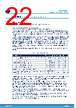
22 / 33 page  7 PCB, BOM, and layout recommendations 7.1 PCB suggestions This section lists some tips to facilitate the PCB routing of the STDRIVEG611. 7.1.1 External BOM values selection and placement A list of recommended value ranges for some key components are reported. The bulk capacitors required for VCC, VCCL, VCCH, and BOOT must be placed as close as possible to relevant pins and relevant references. Such capacitors must be low ESR/ESL ceramic components having rated voltages that are almost twice the maximum operating voltages to overcome the well-known value modulation versus bias voltage. The eventual external bootstrap diode is typically not required in motor control applications but is possible. In case of external diode use, a series resistor with a value of ≥ 2.2 Ω (10 Ω in case of large CBOOT) is recommended to minimize the bootstrap diode peak current, EMI generation and supply rail spike generation. In case an external bootstrap diode is used, the CBOOT capacitor must be placed on the PCB in such a way that the negative terminal is put as close as possible to the OUT pin: this arrangement ensures that the charging current flows in the shortest track possible. In the case of overcurrent comparator use, the user should consider the bootstrap current sums with the load current through the low-side: undesired overcurrent events could be generated especially with low RBOOT values. Turn-on resistors (RONx) need to be placed close to the IC to minimize the length of the track connected to the RONx pin. Table 7. External BOM summary Symbol Function Value (range) Technology Min. rating CVCC VCC large bulk capacitor (it is normally used as bulk capacitor of controller too) 2.2 to 10 µF EL-Cap (or X7R) 25 V VCC bypass capacitor 100 nF X7R 50 V CBOOT BOOT to OUT bypass capacitor CVCCH to 3300 nF X7R 50 V CVCCL VCCL to PGND bypass capacitor 47 nF to 470 nF X7R 16 V CVCCH VCCH to OUT bypass capacitor 47 nF to 470 nF X7R 16 V RBOOT Current limiting resistor of external DBOOT ≥ 2.2 Ω DBOOT External Bootstrap diode (typically not required in motor control applications) STTH1R06 or equivalent Turbofast 600 V / 1 A To speed-up start-up time, the user shall minimize CBOOT and CVCCH values. Most power conversion applications are optimized using CBOOT = CVCCx = 47 nF. Most motor control applications (depending on gate load) are optimized when using CVCCx = 47 to 100 nF and CBOOT = 100 to 470 nF. A larger CBOOT capacitor could be rarely required in specific applications if a very long high side on-time is required. On all other applications is recommended to keep CBOOT small to avoid increasing start-up time, the potential need of the additional external bootstrap diode, the diode dissipation. In extreme cases, as in all gate driver applications, excessive CBOOT and small CVCC can lead to VCC drops due to charge sharing when low- side turns on, detected by the VCC UVLO. PGND must be connected to the low-side GaN (Kelvin if available) source, which creates the path to GND through the optional current shunt resistor. So, PGND shall not be directly connected to GND to avoid shorting the Kelvin connection and reducing its benefits. OUT must be connected to the high-side GaN (Kelvin if available) source. GaN main source and Kelvin source shall not be shorted together externally to best exploit the Kelvin benefits. VCCL and VCCH are the output access to the internal voltage regulator: forcing these pins to external voltage regulators may result in unrecoverable damage of the IC. STDRIVEG611 PCB, BOM, and layout recommendations DS14457 - Rev 2 page 22/33 |
|
链接网址 |
| ALLDATASHEET是否为您带来帮助? [ DONATE ] |
关于 Alldatasheet | 广告服务 | 联系我们 | 隐私政策 | 数据表链接 | 链接交换 | 制造商名单 All Rights Reserved©Alldatasheet.com |
| Russian : Alldatasheetru.com | Korean : Alldatasheet.co.kr | Spanish : Alldatasheet.es | French : Alldatasheet.fr | Italian : Alldatasheetit.com Portuguese : Alldatasheetpt.com | Polish : Alldatasheet.pl | Vietnamese : Alldatasheet.vn Indian : Alldatasheet.in | Mexican : Alldatasheet.com.mx | British : Alldatasheet.co.uk | New Zealand : Alldatasheet.co.nz |
|
Family Site : ic2ic.com |
icmetro.com |
 Chinese ▼
 English
 Chinese
 German
 Japanese
 Russian
 Korean
 Spanish
 French
 Italian
 Portuguese
 Polish
 Vietnamese
 Indian
 Mexican
 British
 New Zealand