|
数据搜索系统,热门电子元器件搜索 |
|
|
数据搜索系统,热门电子元器件搜索 |
|
STDRIVEG611QTR 数据表(PDF) 19 Page - STMicroelectronics |
|
|
|||||||||||||||||||||||||||||
STDRIVEG611QTR 数据表(HTML) 19 Page - STMicroelectronics |
|
|
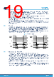
19 / 33 page  High-side regulator input is the BOOT pin; regulator output is the VCCH pin, referred to OUT. Low-ESR ceramic capacitor must be connected as close as possible between VCCH and OUT (CVCCL min. 47 nF, X7R, 16 V) to obtain a clean supply voltage. A slightly higher CVCCH could be required to minimize VHS ripple when driving high GaN QG, but the lower the CVCCH the faster the startup time. Under recommended operating conditions, VCCH regulator can provide an average current of 10 mA. A UVLO on VHS is there to prevent unsafe operations of low-side GaN. When VHS voltage reaches the VHSthON threshold, the high-side driver is enabled to accept turn-on/off commands from the input logic block. When VHS voltage goes below the VHSthOFF threshold, high-side gate driver output is forced low. VHS UVLO status is not signaled on the FLT pin and the low-side driver continues to operate according to inputs and other protections. 6.5 Standby The STDRIVEG611 is designed to reduce the current consumption of both the logic portion and low-side driver when the STBY pin is pulled to GND. Low-side and high-side output are immediately set low to leave the half- bridge in a three-state, while the FLT pin is forced low, and consumption is reduced if the STBY pin is pulled to GND. The overtemperature and the comparator protections are disabled in this operating condition. Setting the STBY pin high, the device wakes up and operation is restored: the FLT pin is released while driver’s outputs are set according to inputs, providing that relevant UVLOs are not active, within tWU. Figure 14. Standby timings LIN OUTL FLT STBY tSTBYoff tSTBY_FLT tWU tWU_FLT HIN OUTH FLT STBY tSTBYoff tSTBY_FLT tWU tWU_FLT 6.6 Comparator with SmartSD The STDRIVEG611 integrates a comparator committed to the fault sensing function. The comparator input can be connected to an external shunt resistor in order to implement a simple overcurrent detection function with an automatic OFF-time mechanism (Smart Shutdown) providing the possibility to increase the disable time after the fault event up to an arbitrary value without increasing the delay time of the protection. The comparator has an internal voltage reference CINth connected to the inverting input, while the non-inverting input is available on the CIN pin. The output signal of the comparator is filtered from glitches shorter than tCINfilter and then fed to the Smart Shutdown logic. The SD/OD is connected to a timing capacitor COD and a pull-up to determine the output disable time of the fault event. When an overcurrent is detected, gates are immediately turned off, the FLT pin is forced low to signal the state to the controller, the SD/OD pin discharges COD down to VSSD and then the external pull-up charges it again. Once COD reaches Vih, the gate driving restarts and FLT is released. STDRIVEG611 Device description DS14457 - Rev 2 page 19/33 |
|
链接网址 |
| ALLDATASHEET是否为您带来帮助? [ DONATE ] |
关于 Alldatasheet | 广告服务 | 联系我们 | 隐私政策 | 数据表链接 | 链接交换 | 制造商名单 All Rights Reserved©Alldatasheet.com |
| Russian : Alldatasheetru.com | Korean : Alldatasheet.co.kr | Spanish : Alldatasheet.es | French : Alldatasheet.fr | Italian : Alldatasheetit.com Portuguese : Alldatasheetpt.com | Polish : Alldatasheet.pl | Vietnamese : Alldatasheet.vn Indian : Alldatasheet.in | Mexican : Alldatasheet.com.mx | British : Alldatasheet.co.uk | New Zealand : Alldatasheet.co.nz |
|
Family Site : ic2ic.com |
icmetro.com |
 Chinese ▼
 English
 Chinese
 German
 Japanese
 Russian
 Korean
 Spanish
 French
 Italian
 Portuguese
 Polish
 Vietnamese
 Indian
 Mexican
 British
 New Zealand