|
数据搜索系统,热门电子元器件搜索 |
|
|
数据搜索系统,热门电子元器件搜索 |
|
STDRIVEG611QTR 数据表(PDF) 16 Page - STMicroelectronics |
|
|
|||||||||||||||||||||||||||||
STDRIVEG611QTR 数据表(HTML) 16 Page - STMicroelectronics |
|
|
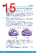
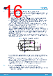
16 / 33 page  6.3.1 Gate driving network for slow hard-off dV/dt (motor control applications) While several applications, typically power conversion, tends to make desirable high dV/dt to minimize switching losses, some others, notably motor control ones, could require limiting dV/dt at the expense of higher switching losses. The main reasons to limit dV/dt in motor control applications are: • EMI control: to pass regulatory emission masks. • Motor winding reliability: especially in high voltage applications with long cables, voltage overshoots on motor poles/winding could generate partial discharge phenomena reducing winding lifetime. • Ball bearing reliability: winding parasitic capacitance to the rotor will generate current peaks during dV/dt toward chassis earth. If those currents flow through classic steel ball bearings, those current can flute bearing rollers and bearing races reducing lifetime. Typically, the EMI point is the bottleneck to limit dV/dt even if the absence of diode recovery with GaN is now pushing higher the dV/dt limit; motor winding and ball bearing issues are seldom, typically found when pushing further dV/dt limit thanks to shorter cables or with specific motors. Hard turn-on dV/dt reduction is an easy task by simply increasing RON resistor. Hard turn-off dV/dt is generally proportional to load parasitic capacitance (the higher the motor parasitic capacitance, the slower the dV/dt). Depending on motor parasitic capacitance and load current, could be required to slow down turn-off. In resonant applications, hard-off dV/dt reduction is typically done by adding a discrete capacitor in parallel to GaN CDS. However, adding this capacitor in hard switching applications leads to increase hard-on switching losses loosing some GaN benefits. In motor control applications with MOSFETs, hard turn-off slow down is typically done by increasing the turn-off resistor. However with GaN this could easily lead to induced turn-on phenomenon unless a specific gate driving network is used as the following one. Figure 12. Hard-off dV/dt limiting gate driving network Driver VCCx RONx OUTx PGND/OUT RON CVCCx GATE R CGM CGS CGD While the GaN is off and during dV/dt generated by the companion GaN, CGD charges CGS. If RGATE has a high value, due to requirement to slow down hard-off dV/dt, VGS could easily exceed VGSth leading to induced turn-on phenomenon. The higher the CGD/CGS ratio and the lower the VGSth, the most likely the induced turn-on could occur. Adding the CGM capacitor, the overall CGD/CGS ratio decreases avoiding the induced turn-on phenomenon and enabling hard-off dV/dt reduction increasing RGATE. The CGM capacitor required to use this technique depends on several factors like GaN characteristics, bus voltage and load current but, as a rule-of-thumb, it is in the range around 3-5 times QGS/VGSth. 6.4 Supply rails, LDOs, UVLO protections, and bootstrap diode The STDRIVEG611 is supplied by two rails: VCC, referred to GND, and BOOT referred to OUT. Integrated LDOs generate supply voltages for low-side and high-side output stages (VLS and VHS). Undervoltage circuitries monitor VCC, VLS and VHS. STDRIVEG611 Device description DS14457 - Rev 2 page 16/33 |
|
链接网址 |
| ALLDATASHEET是否为您带来帮助? [ DONATE ] |
关于 Alldatasheet | 广告服务 | 联系我们 | 隐私政策 | 数据表链接 | 链接交换 | 制造商名单 All Rights Reserved©Alldatasheet.com |
| Russian : Alldatasheetru.com | Korean : Alldatasheet.co.kr | Spanish : Alldatasheet.es | French : Alldatasheet.fr | Italian : Alldatasheetit.com Portuguese : Alldatasheetpt.com | Polish : Alldatasheet.pl | Vietnamese : Alldatasheet.vn Indian : Alldatasheet.in | Mexican : Alldatasheet.com.mx | British : Alldatasheet.co.uk | New Zealand : Alldatasheet.co.nz |
|
Family Site : ic2ic.com |
icmetro.com |
 Chinese ▼
 English
 Chinese
 German
 Japanese
 Russian
 Korean
 Spanish
 French
 Italian
 Portuguese
 Polish
 Vietnamese
 Indian
 Mexican
 British
 New Zealand