|
数据搜索系统,热门电子元器件搜索 |
|
|
数据搜索系统,热门电子元器件搜索 |
|
FT600Q-B-R 数据表(PDF) 11 Page - Future Technology Devices International Ltd. |
|
|
|||||||||||||||||||||||||||||
FT600Q-B-R 数据表(HTML) 11 Page - Future Technology Devices International Ltd. |
|
|
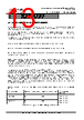
11 / 33 page  Copyright © Future Technology Devices International Limited 11 FT600Q-FT601Q IC DatasheetDatasheet Version 1.04 Document No.: FT_001118 Clearance No.: FTDI#424 4 Function Description FT60x is a high performance USB 3.0-to-FIFO interface bridge chip. This device can be used in those applications which require high data throughput such as imaging devices and Multi-Channel FIFO ADC or DAC devices etc. The FIFO interface can support multi-voltage I/O (1.8V, 2.5V, 3.3V) and operating frequencies of 66.67MHz or 100MHz. 100MHz only for 2.5V and 3.3V. There are 2 different proprietary synchronous bus protocols supported; one FIFO bus protocol is called the “Multi-Channel FIFO” bus protocol and the other is the “245 Synchronous FIFO” bus protocol. The latter being an extension of the interface introduced in the FT232H/FT2232H devices. 4.1 Key Features and Function Description Functional Integration. The following features are integral to the IC design: FIFO protocol management, USB 3.0 controller, USB3.0 and USB2.0 PHYs, GPIOs, power management, clock generation, power-on-reset (POR) and LDO regulator. USB 3.0 Protocol Controller. The USB 3.0 Protocol Controller manages the data stream from the device USB control endpoint. It handles the USB protocol requests generated by the USB host controller and the commands for controlling the functional parameters of the FIFO in accordance with the USB 3.0 specification. FIFO Management. This unit is used to manage all PIPE data or buffers in the FIFO memory; the data is sent or received through the FIFO protocol layer. Through this block the FIFO memory can be allocated to each PIPE with any size of memory as long as the total memory allocated to all PIPEs does not exceed the maximum FIFO memory size which is 16KB. Additionally, the FIFO signals have a configurable high drive strength capability and can be set to 18Ω, 25Ω, 35Ω and 50Ω. Multi-Channel FIFO Bus protocol. The multi-Channel FIFO bus is a slave bus and is designed to handle Multi-Channel FIFO connectivity. The bus protocol supports a total of 8 channels (4 INs and 4 OUTs). CLK is the clock output to the FIFO bus master. 245 Synchronous FIFO Bus protocol. The 245 Synchronous FIFO bus is a slave bus with one IN and one OUT FIFO channel supported by this bus protocol. CLK is the clock output to the FIFO bus master. FIFO Bus Clock Option. The device provides the following FIFO bus clock frequency option: 100MHz. FIFO RX/TX Buffer (16k bytes). Data sent from the USB host controller to the FIFO via the USB data OUT endpoint is stored in the FIFO RX (receive) buffer and is removed from the buffer by reading the contents of the FIFO using the RD# pin. (RX relative to the USB interface). |
|
链接网址 |
| ALLDATASHEET是否为您带来帮助? [ DONATE ] |
关于 Alldatasheet | 广告服务 | 联系我们 | 隐私政策 | 数据表链接 | 链接交换 | 制造商名单 All Rights Reserved©Alldatasheet.com |
| Russian : Alldatasheetru.com | Korean : Alldatasheet.co.kr | Spanish : Alldatasheet.es | French : Alldatasheet.fr | Italian : Alldatasheetit.com Portuguese : Alldatasheetpt.com | Polish : Alldatasheet.pl | Vietnamese : Alldatasheet.vn Indian : Alldatasheet.in | Mexican : Alldatasheet.com.mx | British : Alldatasheet.co.uk | New Zealand : Alldatasheet.co.nz |
|
Family Site : ic2ic.com |
icmetro.com |
 Chinese ▼
 English
 Chinese
 German
 Japanese
 Russian
 Korean
 Spanish
 French
 Italian
 Portuguese
 Polish
 Vietnamese
 Indian
 Mexican
 British
 New Zealand