|
数据搜索系统,热门电子元器件搜索 |
|
|
数据搜索系统,热门电子元器件搜索 |
|
ADP2116ACPZ-R7 数据表(PDF) 21 Page - Analog Devices |
|
|
|||||||||||||||||||||||||||||
ADP2116ACPZ-R7 数据表(HTML) 21 Page - Analog Devices |
|
|
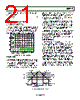
21 / 36 page  ADP2116 Rev. 0 | Page 21 of 36 The capacitance value of the soft start capacitor defines the soft start time, tSS, based on SS SS SS REF C I t V = (1) where: VREF is the internal reference voltage, 0.6 V. ISS is the soft start current, 6 μA. CSS is the soft start capacitor value. If the output voltage, VOUT1 or VOUT2, is precharged prior to enabling Channel 1 or Channel 2, respectively, the control logic prevents inductor current reversal by keeping the power MOSFETs turned off until the soft start voltage ramp at SS1 or SS2 reaches the precharged output voltage on VFB1 or VFB2 (see Figure 59). CH3 5.0V CH2 1.0V CH1 5.0V CH4 500mV M200µs 50MS/s A CH1 2.4V 1 2 4 3 EN1 VOUT1 SS1 SW1, SW2 20ns/pt B W B W B W B W Figure 59. Soft Start with a Precharged Output POWER GOOD The ADP2116 features open-drain power-good outputs (PGOOD1 and PGOOD2) that indicate when the converter output voltage is within regulation. The power-good signal transitions low immediately when the corresponding channel is disabled. The power-good circuitry monitors the output voltage on the FB1 or FB2 pin and compares it to the rising and falling thresholds specified in Table 1. If the rising output voltage (VOUT1 or VOUT2) exceeds 116% of the target output voltage (VOUT1SET or VOUT2SET), the PGOOD1 or PGOOD2 pin is held low. The PGOOD1 or PGOOD2 pin continues to be held low until the falling output voltage returns to 108% of the target value. If the output voltage drops below 84% of the target output voltage, the corresponding PGOOD1 or PGOOD2 pin is held low. The PGOOD1 or PGOOD2 pin continues to be held low until the output voltage rises to within 92% of the target output voltage. The PGOOD1 or PGOOD2 pin is then released, signaling that the output voltage is within the power-good window. The power-good thresholds are shown in Figure 60. The PGOOD1 and PGOOD2 outputs also sink current if an overtemperature condition is detected. Use these outputs as logic power-good signals by connecting the pull-up resistor from PGOOD1 or PGOOD2 to VDD. If the power-good function is not used, the pins can be left floating. PULSE SKIP MODE The ADP2116 has built-in pulse skip circuitry that turns on during light loads, switching only as necessary to maintain the output voltage within regulation. This allows the converter to maintain high efficiency during light load operation by reducing the switching losses. The pulse skip mode can be selected by configuring the OPCFG pin as indicated in Table 7. In pulse skip mode, when the output voltage dips below regulation, the ADP2116 enters PWM mode for a few oscillator cycles to increase the output voltage so that it is within regulation. During the wait time between bursts, both power switches are off, and the output capacitor supplies all of the load current. Because the output voltage dips and recovers occasionally, the output voltage ripple in this mode is larger than the ripple in the PWM mode of operation. If the converter is configured to operate in forced PWM mode (by selecting this configuration using the OPCFG pin), the device operates with a fixed switching frequency, even at light loads. 108% 92% 116% 84% 100% 100% PGOOD1/PGOOD2 VOUT FALLING VOUT RISING POWER GOOD OVERVOLTAGE UNDERVOLTAGE UNDERVOLTAGE POWER GOOD Figure 60. PGOOD1/PGOOD2 Thresholds |
|
链接网址 |
| ALLDATASHEET是否为您带来帮助? [ DONATE ] |
关于 Alldatasheet | 广告服务 | 联系我们 | 隐私政策 | 数据表链接 | 链接交换 | 制造商名单 All Rights Reserved©Alldatasheet.com |
| Russian : Alldatasheetru.com | Korean : Alldatasheet.co.kr | Spanish : Alldatasheet.es | French : Alldatasheet.fr | Italian : Alldatasheetit.com Portuguese : Alldatasheetpt.com | Polish : Alldatasheet.pl | Vietnamese : Alldatasheet.vn Indian : Alldatasheet.in | Mexican : Alldatasheet.com.mx | British : Alldatasheet.co.uk | New Zealand : Alldatasheet.co.nz |
|
Family Site : ic2ic.com |
icmetro.com |
 Chinese ▼
 English
 Chinese
 German
 Japanese
 Russian
 Korean
 Spanish
 French
 Italian
 Portuguese
 Polish
 Vietnamese
 Indian
 Mexican
 British
 New Zealand