|
数据搜索系统,热门电子元器件搜索 |
|
|
数据搜索系统,热门电子元器件搜索 |
|
AM2434...ALV 数据表(PDF) 8 Page - Texas Instruments |
|
|
|||||||||||||||||||||||||||||
AM2434...ALV 数据表(HTML) 8 Page - Texas Instruments |
|
|
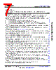
8 / 280 page  • (Pin Attributes - ALV Pins D10 E10 - ALX Pins C5 B3): DSIS values for the EMU[1:0] pins were defined to be “1”. ................................................................................................................................................................... 20 • (USB Signal Descriptions): Added USB0_RCALIB 7.2mW maximum power dissipation and updated calibration resistor value from 500 Ω ±1% to 499 Ω ±1%................................................................................. 20 • (Pin Attributes - ALV Pins C20 D19 - ALX Pins C16 B17): DSIS values for the MMC1_SDCD and MCC1_SDWP pins were changed from “1” to “0”. ..........................................................................................20 • (Signal Description Header List): Added "OD" signal type and direction..........................................................71 • (ADC0 Signal Descriptions): Added the ADC0_REFP and ADC0_REFN signals and included a note that describes connectivity expectations for these analog inputs............................................................................ 71 • (ADC0 Signal Descriptions): Added a note and note references to identify each GPI with a debounce function ..........................................................................................................................................................................71 • (ADC0 Signal Descriptions): Added a note that clarifies ADC0_AIN[7:0] inputs only have hysterisis when ADC0 is configured to operate in GPI mode ....................................................................................................71 • (ADC0 Signal Descriptions): Added a note that clarifies connectivity expectations for unused ADC0_AIN[7:0] inputs................................................................................................................................................................ 71 • (GPIO1 Signal Descriptions): Added a note and note references to identify each GPIO with a debounce function............................................................................................................................................................. 71 • (GPIO1 Signal Descriptions): Changed the PIN TYPE value of GPIO1_64, GPIO1_65, and GPIO1_70 from "IO" to "IOD" since the IOs associated with these signals have an open-drain output.....................................71 • (MCU_GPIO0 Signal Descriptions): Added a note and note references to identify each GPIO with debounce function............................................................................................................................................................. 71 • (MCU_GPIO0 Signal Descriptions): Changed the PIN TYPE value of MCU_GPIO1_18 and MCU_GPIO1_19 from "IO" to "IOD" since the IO associated with these signals have an open-drain output...............................71 • (Power Supply Signal Descriptions): Removed J15 from the list of VDDS_MMC0 pins and K16 from the list of VSS pins........................................................................................................................................................... 71 • (UART6 Signal Descriptions): Removed pin A18 from the list of UART6_CTSn pins and removed pin B18 from the list of UART6_RTSn pins....................................................................................................................71 • (USB0 Signal Descriptions): Update the calibration resistor value in the note to a standard 1% value and defined the maximum power dissipation expected for this resistor.................................................................. 71 • (Pin Connectivity Requirements): Included VMON connectivity requirements............................................... 109 • (Pin Connectivity Requirements): Included ADC0_REFP and ADC0_REFN connectivity requirements when ADC0 is not used............................................................................................................................................109 • (Pin Connectivity Requirements): Deleted pin J15 from the row associated with VDDS_MMC0................... 109 • (Absolute Maximum Ratings): Defined remaining TBD values....................................................................... 115 • (Absolute Maximum Ratings): Changed MCU_PORz maximum value from 2.2 V to 3.63 V......................... 115 • (Absolute Maximum Ratings): Changed all 2.2 V maximum values to 1.98 V................................................115 • (Absolute Maximum Ratings): Changed all 3.8 V maximum values to 3.63 V................................................115 • (Absolute Maximum Ratings): Updated the "Operation outside the Absolute Maximum Ratings may cause …" disclaimer footnote..........................................................................................................................................115 • (Absolute Maximum Ratings): Added USB0_ID and associated note to define its absolute maximum ratings.... 115 • Added VMON_VSYS to the paragraph that is describing Fail-safe IO terminals............................................115 • (ESD Ratings): Replaced TBD values with tested values...............................................................................117 • (Power-On Hours (POH)): Added Estimated Lifetime POH table and associated app note links...................118 • (Power-On Hours (POH)): Adding POH details for Extended Industrial temperature range...........................118 • (Recommended Operating Conditions): Adding row for VDDS_MMC0 and USB0_ID...................................119 • Updated TJ to include Extended Industrial operating junction temperature range..........................................119 • (I2C OD FS Electrical Characteristics): Added a note to explain the IOL parameter.......................................122 • (I2C OD FS Electrical Characteristics): Defined maximum VIH values for 1.8-V mode and 3.3-V mode and included a note that describes how these values also define the absolute maximum input voltage. Removed the typical Input Leakage Current value and several TBD values which were not applicable........................122 • (I2C OD FS Electrical Characteristics): Removed the typical Input Leakage Current value and several TBD values which were not applicable................................................................................................................... 122 • (I2C OD FS Electrical Characteristics): Defined the minimum input slew rate value and added notes to describe this parameter.................................................................................................................................. 122 AM2434, AM2432, AM2431 SPRSP65D – APRIL 2021 – REVISED AUGUST 2022 www.ti.com 8 Submit Document Feedback Copyright © 2022 Texas Instruments Incorporated Product Folder Links: AM2434 AM2432 AM2431 |
|
链接网址 |
| ALLDATASHEET是否为您带来帮助? [ DONATE ] |
关于 Alldatasheet | 广告服务 | 联系我们 | 隐私政策 | 数据表链接 | 链接交换 | 制造商名单 All Rights Reserved©Alldatasheet.com |
| Russian : Alldatasheetru.com | Korean : Alldatasheet.co.kr | Spanish : Alldatasheet.es | French : Alldatasheet.fr | Italian : Alldatasheetit.com Portuguese : Alldatasheetpt.com | Polish : Alldatasheet.pl | Vietnamese : Alldatasheet.vn Indian : Alldatasheet.in | Mexican : Alldatasheet.com.mx | British : Alldatasheet.co.uk | New Zealand : Alldatasheet.co.nz |
|
Family Site : ic2ic.com |
icmetro.com |
 Chinese ▼
 English
 Chinese
 German
 Japanese
 Russian
 Korean
 Spanish
 French
 Italian
 Portuguese
 Polish
 Vietnamese
 Indian
 Mexican
 British
 New Zealand