|
数据搜索系统,热门电子元器件搜索 |
|
|
数据搜索系统,热门电子元器件搜索 |
|
P9415-R 数据表(PDF) 9 Page - Renesas Technology Corp |
|
|
|||||||||||||||||||||||||||||
P9415-R 数据表(HTML) 9 Page - Renesas Technology Corp |
|
|
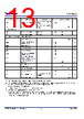
9 / 62 page  P9415-R Datasheet © 2021 Renesas Electronics Corporation 9 May 4, 2021 Pin Number Name Type Description D2 GP5 / INHIBIT I/O General Purpose Push-Pull I/O, referenced to LDO1P8. When this pin is LOW, Rx mode is turned on. When it is HIGH, the P9415-R cannot go into Rx mode. If this pin is driven high in the power transfer phase, an EPT will be sent to the TX. VRECT protection is ON in INHIBIT mode. If not used, connect this pin to GND (INHIBIT). This pin is not used in Tx mode. D3 PCLAMP I High voltage open-drain input for linear clamping during OVP events. Connect a resistor from this pin to VRECT for > 5W operation. Short directly to VRECT for 5W or lower power applications. D4 GP3 / Q_OFFSET I/O General Purpose Push-Pull I/O, referenced to LDO1P8. This pin is used to set the default Q factor reported in the EPP mode. Default Q factor = Q factor main (based on GP1 voltage) + Q factor offset (based on GP3 voltage). To use the firmware default Q factor, connect this pin to GND. D5 GP6 / EPP_DISABLE I/O General Purpose Push-Pull I/O, referenced to LDO1P8. When this pin is HIGH, Rx EPP mode is disabled and the P9415-R operates in BPP mode. Connect this pin to GND to enable EPP mode by default. D6 LDO1P8 O 1.8V LDO for Internal Core (always on when VRECT is powered). Connect a capacitor to the ground. E1, E2, E3, E5, E6 VOUT O Main LDO output pin. Connect a capacitor to the ground. Connect an external voltage to this pin in Tx mode. E4 OUT_S I Optional output voltage sensing pin. Connect this pin to VOUT pins. F1, F2, F3, F4, F5, F6 VRECT O Filter cap for the internal rectifier output. Connect a capacitor to the ground. G1 BST1 O Bootstrap capacitor for driving high side N-MOSFET of the internal rectifier. Connect a capacitor from AC1 to BST1. G2, H1, H2, H3 AC1 I/O Connect to the RX LC tank (due to symmetry may connect to Rx coil or Resonance Capacitor). G3 nEN I Active-low enable pin. When it is pulled-up High by the AP GPIO, the rectifier will be set in Diode mode without ASK signal modulation and the P9415-R is not enabled. While it is pulled-down Low, the rectifier can be set in any predefined modes. G5, H4, H5, H6 AC2 I/O Connect to the RX LC tank (due to symmetry may connect to Rx coil or Resonance Capacitor). G4 DEMOD I Tx mode Communication Demodulator input. Connect to LC node via diode and DEMOD filter. This pin can be left floating if TRx mode is not used. G6 BST2 O Bootstrap capacitor for driving the high side N-MOSFET of the internal rectifier. Connect a capacitor from AC2 to BST2. C1, C2, C6, J1, J2, J3, J4, J5, J6 PGND GND Power Ground. All PGND pins must be connected tied together externally. [a] Note: I = Input (Digital or Analog), O = Output (Digital). |
|
链接网址 |
| ALLDATASHEET是否为您带来帮助? [ DONATE ] |
关于 Alldatasheet | 广告服务 | 联系我们 | 隐私政策 | 数据表链接 | 链接交换 | 制造商名单 All Rights Reserved©Alldatasheet.com |
| Russian : Alldatasheetru.com | Korean : Alldatasheet.co.kr | Spanish : Alldatasheet.es | French : Alldatasheet.fr | Italian : Alldatasheetit.com Portuguese : Alldatasheetpt.com | Polish : Alldatasheet.pl | Vietnamese : Alldatasheet.vn Indian : Alldatasheet.in | Mexican : Alldatasheet.com.mx | British : Alldatasheet.co.uk | New Zealand : Alldatasheet.co.nz |
|
Family Site : ic2ic.com |
icmetro.com |
 Chinese ▼
 English
 Chinese
 German
 Japanese
 Russian
 Korean
 Spanish
 French
 Italian
 Portuguese
 Polish
 Vietnamese
 Indian
 Mexican
 British
 New Zealand