|
数据搜索系统,热门电子元器件搜索 |
|
|
数据搜索系统,热门电子元器件搜索 |
|
STV-6410-R01 数据表(PDF) 70 Page - STMicroelectronics |
|
|
|||||||||||||||||||||||||||||
STV-6410-R01 数据表(HTML) 70 Page - STMicroelectronics |
|
|
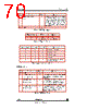
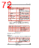
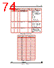
70 / 105 page  VV5410 & VV6410 Serial Control Bus cd5410-6410f-3-0.fm Commercial in confidence 70/105 [22], [16] - data_format 5 Enable RESETB pin as SIN Off / On 0 On power up the RESETB pin is configured as an active low system reset which will synchronise the video timing logic and reset all serial registers to their default state. Setting this bit configures the RESETB pin as an active high system synchronisation signal (SIN) which will synchronise the video timing but will NOT reset the serial registers. 7:6 unused 0 Mapping Enable FST pin QCK pin 0 FST QCK 1 pin_mapping[2] pin_mapping[1] Table 38 : FST/QCK Pin Selection oeb_composite pin_map[4] pin_map[3] Comments 0 0 0 Drive strength = 2mA (Default) 0 0 1 Drive strength = 4mA 0 1 0 Drive strength = 6mA 0 1 1 unallocated 1 x x Outputs are not being driven therefore driver strength is irrelevant Table 39 : Output driver strength selection Bit Function Default Comment 1:0 Unused 1 2 Line read-out order (vertical) Unshuffled or Shuffled 0 If the line read out is shuffled then all the even address rows will be read out first followed by all the odd address rows 3 Pixel read-out order (hmirror) Normal or Mirrored 0 If the pixel read out is horizontally mirrored then the columns are read out in reverse order, that is the column on the right of the sensor array will appear on the left of the displayed image and vice versa 4 Line read-out order (vertical flip) Normal or Mirrored 0 If the line read out is vertically mirrored then the rows are read out in reverse order, that is the row at the bottom of the array will appear at the top of the displayed image and vice versa. Table 40 : [22], [16] - data_format Bit Function Default Comment Table 37 : [21], [15] - pin_mapping |
|
链接网址 |
| ALLDATASHEET是否为您带来帮助? [ DONATE ] |
关于 Alldatasheet | 广告服务 | 联系我们 | 隐私政策 | 数据表链接 | 链接交换 | 制造商名单 All Rights Reserved©Alldatasheet.com |
| Russian : Alldatasheetru.com | Korean : Alldatasheet.co.kr | Spanish : Alldatasheet.es | French : Alldatasheet.fr | Italian : Alldatasheetit.com Portuguese : Alldatasheetpt.com | Polish : Alldatasheet.pl | Vietnamese : Alldatasheet.vn Indian : Alldatasheet.in | Mexican : Alldatasheet.com.mx | British : Alldatasheet.co.uk | New Zealand : Alldatasheet.co.nz |
|
Family Site : ic2ic.com |
icmetro.com |
 Chinese ▼
 English
 Chinese
 German
 Japanese
 Russian
 Korean
 Spanish
 French
 Italian
 Portuguese
 Polish
 Vietnamese
 Indian
 Mexican
 British
 New Zealand