|
数据搜索系统,热门电子元器件搜索 |
|
|
数据搜索系统,热门电子元器件搜索 |
|
SSM2602CPZ-R2 数据表(PDF) 14 Page - Analog Devices |
|
|
|||||||||||||||||||||||||||||
SSM2602CPZ-R2 数据表(HTML) 14 Page - Analog Devices |
|
|
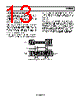
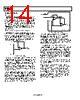
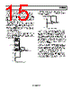
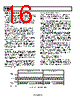
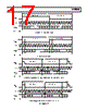
14 / 32 page  SSM2602 Rev. 0 | Page 14 of 32 ANALOG INTERFACE Signal Chain The SSM2602 includes stereo single-ended line and monaural microphone inputs to the on-board ADC. Either the line inputs or the microphone input, but not both simultaneously, can be connected to the ADC by setting the INSEL bit (Register R4, Bit D2). In addition, the line or microphone inputs can be routed and mixed directly to the output terminals via the SIDETONE_EN (Register R4, Bit D5) and BYPASS (Register R4, Bit D3) bits. The SSM2602 also includes line and headphone outputs from the on-board DAC. Stereo Line and Monaural Microphone Inputs The SSM2602 contains a set of single-ended stereo line inputs (RLINEIN and LLINEIN) that are internally biased to VMID by way of a voltage divider between AVDD and AGND. The line input signal can be connected to the internal ADC and, if desired, routed directly to the outputs via the bypass path by using the BYPASS bit (Register R4, Bit D3). ADC OR BYPASS LINEIN AVDD VMID AGND + – Figure 19. Line Input to ADC The line input volume can be adjusted from −34.5 dB to +33 dB in steps of +1.5 dB by setting the LINVOL (Register R0, Bit D0 to Bit D5) and RINVOL (Register R1, Bit D0 to Bit D5) bits. Volume control, by default, is independently adjustable on both right and left line inputs. However, the LRINBOTH or RLINBOTH bit, if selected, simultaneously loads both sets of volume control with the same value. The user can also set the LINMUTE (Register R0, Bit D7) and RINMUTE (Register R1, Bit D7) bits to mute the line input signal to the ADC. The high impedance, low capacitance monaural microphone input pin (MICIN) has two gain stages and a microphone bias level (MICBIAS) that is internally biased to the VMID voltage level by way of a voltage divider between AVDD and AGND. The microphone input signal can be connected to the internal ADC and, if desired, routed directly to the outputs via the sidetone path by using the SIDETONE_EN bit (Register R4, Bit D5). ADC OR SIDETONE INTERNAL CIRCUITRY MICIN AVDD VMID AGND REXT GAIN = 50kΩ (REXT + 10kΩ) 10kΩ 50kΩ 0Ω/20dB/40dB GAIN BOOST Figure 20. Microphone Input to ADC The first gain stage is composed of a low noise operational amplifier set to an inverting configuration with integrated 50 kΩ feedback and 10 kΩ input resistors. The default microphone input signal gain is 14 dB. An external resistor (REXT) can be connected in series with the MICIN pin to reduce the first-stage gain of the microphone input signal to as low as 0 dB by using the following equation: Microphone Input Gain = 50 kΩ/(10 kΩ + REXT) The second-stage gain of the microphone signal path is derived from the internal microphone boost circuitry. The available settings are 0 dB, 20 dB, and 40 dB and are controlled by the MICBOOST (Register R4, Bit D0) and MICBOOST2 (Register R4, Bit D8) bits. To achieve 20 dB of secondary gain boost, the user can select either MICBOOST or MICBOOST2. To achieve 40 dB of secondary microphone signal gain, the user must select both MICBOOST and MICBOOST2. In similar functionality to the line inputs, the user can set the MUTEMIC bit (Register R4, Bit D1) to mute the microphone input signal to the ADC. Note that when sourcing audio data from both line and microphone inputs, the maximum full-scale input of the ADC is 1.0 V rms when AVDD = 3.3 V. Do not source any input voltage larger than full scale to avoid overloading the ADC, which causes distortion of sound and deterioration of audio quality. For best sound quality in both microphone and line inputs, gain should be carefully configured so that the ADC receives a signal equal to its full scale. This maximizes the signal-to-noise ratio for best total audio quality. |
|
链接网址 |
| ALLDATASHEET是否为您带来帮助? [ DONATE ] |
关于 Alldatasheet | 广告服务 | 联系我们 | 隐私政策 | 数据表链接 | 链接交换 | 制造商名单 All Rights Reserved©Alldatasheet.com |
| Russian : Alldatasheetru.com | Korean : Alldatasheet.co.kr | Spanish : Alldatasheet.es | French : Alldatasheet.fr | Italian : Alldatasheetit.com Portuguese : Alldatasheetpt.com | Polish : Alldatasheet.pl | Vietnamese : Alldatasheet.vn Indian : Alldatasheet.in | Mexican : Alldatasheet.com.mx | British : Alldatasheet.co.uk | New Zealand : Alldatasheet.co.nz |
|
Family Site : ic2ic.com |
icmetro.com |
 Chinese ▼
 English
 Chinese
 German
 Japanese
 Russian
 Korean
 Spanish
 French
 Italian
 Portuguese
 Polish
 Vietnamese
 Indian
 Mexican
 British
 New Zealand