|
数据搜索系统,热门电子元器件搜索 |
|
|
数据搜索系统,热门电子元器件搜索 |
|
SSM2602CPZ-R2 数据表(PDF) 18 Page - Analog Devices |
|
|
|||||||||||||||||||||||||||||
SSM2602CPZ-R2 数据表(HTML) 18 Page - Analog Devices |
|
|
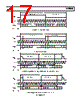
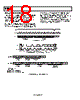
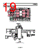
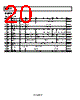
18 / 32 page  SSM2602 Rev. 0 | Page 18 of 32 SOFTWARE CONTROL INTERFACE The software control interface provides access to the user-selectable control registers and can operate with a 2-wire (I2C) or 3-wire (SPI) interface, depending on the setting of the MODE pin. If the MODE pin is set to 0, the 2-wire interface is selected; if 1, the 3-wire interface is selected. Within each control register is a control data-word consisting of 16 bits, MSB first. Bit B15 to Bit B9 are the register map address, and Bit B8 to Bit B0 are register data for the associated register map. When 2-wire (I2C) mode is selected, SDIN generates the serial control data-word, SCLK clocks the serial data, and CSB determines the I2C device address. If the CSB pin is set to 0, the address selected is 0011010; if 1, the address is 0011011. When 3-wire (SPI) mode is selected, SDIN generates the control data-word, SCLK clocks the control data-word into the SSM2602, and CSB latches in the control data-word. B15 B14 CSB SCLK SDIN B0 B01 B02 B03 B04 B05 B06 B07 B08 B09 B10 B11 B12 B13 REGISTER MAP ADDRESS REGISTER DATA Figure 28. SPI Serial Interface P 9 8 1 – 7 9 8 1 – 7 9 8 1 – 7 S SDIN SCLK START ADDR R/W ACK ACK SUBADDRESS ACK STOP DATA Figure 29. SSM2602 2-Wire I2C Generalized Clocking Diagram WRITE SEQUENCE READ SEQUENCE SA1 A7 A0 A(S) A(S) S B15 B9 0 01 0P 0 ... A1 A7 A0 A(S) ... B0 B8 B7 A(M) A(M) ... B0 B7 P ... ... ... DEVICE ADDRESS DEVICE ADDRESS REGISTER ADDRESS SA1 A7 A0 A(S) A(S) A(S) B15 B9 B8 0 ... ... DEVICE ADDRESS REGISTER ADDRESS REGISTER DATA (SLAVE DRIVE) REGISTER DATA S/P = START/STOP BIT. A0 = I2C R/W BIT. A(S) = ACKNOWLEDGE BY SLAVE. A(M) = ACKNOWLEDGE BY MASTER. A(M) = ACKNOWLEDGE BY MASTER (INVERSION). Figure 30. SSM2602 I2C Write and Read Sequences |
|
链接网址 |
| ALLDATASHEET是否为您带来帮助? [ DONATE ] |
关于 Alldatasheet | 广告服务 | 联系我们 | 隐私政策 | 数据表链接 | 链接交换 | 制造商名单 All Rights Reserved©Alldatasheet.com |
| Russian : Alldatasheetru.com | Korean : Alldatasheet.co.kr | Spanish : Alldatasheet.es | French : Alldatasheet.fr | Italian : Alldatasheetit.com Portuguese : Alldatasheetpt.com | Polish : Alldatasheet.pl | Vietnamese : Alldatasheet.vn Indian : Alldatasheet.in | Mexican : Alldatasheet.com.mx | British : Alldatasheet.co.uk | New Zealand : Alldatasheet.co.nz |
|
Family Site : ic2ic.com |
icmetro.com |
 Chinese ▼
 English
 Chinese
 German
 Japanese
 Russian
 Korean
 Spanish
 French
 Italian
 Portuguese
 Polish
 Vietnamese
 Indian
 Mexican
 British
 New Zealand