|
数据搜索系统,热门电子元器件搜索 |
|
|
数据搜索系统,热门电子元器件搜索 |
|
EPF10K100 数据表(PDF) 37 Page - Altera Corporation |
|
|
|||||||||||||||||||||||||||||
EPF10K100 数据表(HTML) 37 Page - Altera Corporation |
|
|
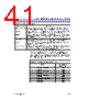
37 / 128 page  Altera Corporation 37 FLEX 10K Embedded Programmable Logic Device Family Data Sheet ClockLock & ClockBoost Features To support high-speed designs, selected FLEX 10K devices offer optional ClockLock and ClockBoost circuitry containing a phase-locked loop (PLL) that is used to increase design speed and reduce resource usage. The ClockLock circuitry uses a synchronizing PLL that reduces the clock delay and skew within a device. This reduction minimizes clock-to-output and setup times while maintaining zero hold times. The ClockBoost circuitry, which provides a clock multiplier, allows the designer to enhance device area efficiency by sharing resources within the device. The ClockBoost feature allows the designer to distribute a low-speed clock and multiply that clock on-device. Combined, the ClockLock and ClockBoost features provide significant improvements in system performance and bandwidth. The ClockLock and ClockBoost features in FLEX 10K devices are enabled through the Altera software. External devices are not required to use these features. The output of the ClockLock and ClockBoost circuits is not available at any of the device pins. The ClockLock and ClockBoost circuitry locks onto the rising edge of the incoming clock. The circuit output can only drive the clock inputs of registers; the generated clock cannot be gated or inverted. The dedicated clock pin (GCLK1) supplies the clock to the ClockLock and ClockBoost circuitry. When the dedicated clock pin is driving the ClockLock or ClockBoost circuitry, it cannot drive elsewhere in the device. In designs that require both a multiplied and non-multiplied clock, the clock trace on the board can be connected to GCLK1. With the Altera software, GCLK1 can feed both the ClockLock and ClockBoost circuitry in the FLEX 10K device. However, when both circuits are used, the other clock pin (GCLK0) cannot be used. Figure 17 shows a block diagram of how to enable both the ClockLock and ClockBoost circuits in the Altera software. The example shown is a schematic, but a similar approach applies for designs created in AHDL, VHDL, and Verilog HDL. When the ClockLock and ClockBoost circuits are used simultaneously, the input frequency parameter must be the same for both circuits. In Figure 17, the input frequency must meet the requirements specified when the ClockBoost multiplication factor is two. |
|
链接网址 |
| ALLDATASHEET是否为您带来帮助? [ DONATE ] |
关于 Alldatasheet | 广告服务 | 联系我们 | 隐私政策 | 数据表链接 | 链接交换 | 制造商名单 All Rights Reserved©Alldatasheet.com |
| Russian : Alldatasheetru.com | Korean : Alldatasheet.co.kr | Spanish : Alldatasheet.es | French : Alldatasheet.fr | Italian : Alldatasheetit.com Portuguese : Alldatasheetpt.com | Polish : Alldatasheet.pl | Vietnamese : Alldatasheet.vn Indian : Alldatasheet.in | Mexican : Alldatasheet.com.mx | British : Alldatasheet.co.uk | New Zealand : Alldatasheet.co.nz |
|
Family Site : ic2ic.com |
icmetro.com |
 Chinese ▼
 English
 Chinese
 German
 Japanese
 Russian
 Korean
 Spanish
 French
 Italian
 Portuguese
 Polish
 Vietnamese
 Indian
 Mexican
 British
 New Zealand