|
数据搜索系统,热门电子元器件搜索 |
|
|
数据搜索系统,热门电子元器件搜索 |
|
MPZ2012S221A 数据表(PDF) 54 Page - STMicroelectronics |
|
|
|||||||||||||||||||||||||||||
MPZ2012S221A 数据表(HTML) 54 Page - STMicroelectronics |
|
|
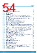
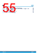
54 / 56 page  List of figures Figure 1. Pin connection (top view) ............................................................. 2 Figure 2. Basic application................................................................... 4 Figure 3. Frequency setting with dithering (left) and without (right) ....................................... 8 Figure 4. Iso-buck general schematic ........................................................... 9 Figure 5. Block diagram ................................................................... 10 Figure 6. Power-up/down procedure ........................................................... 11 Figure 7. Soft-start procedure ............................................................... 12 Figure 8. Tracked soft-start at secondary side .................................................... 12 Figure 9. Simulation with different masking times: insufficient (< 100 ns, left) and appropriate (390 ns, right) ......... 13 Figure 10. Remaining oscillations (left) and their filtering with RC snubber (right) VIN = 12 V, N = 6, IOUTiso = 200 mA .... 13 Figure 11. Switch-over selection............................................................... 14 Figure 12. Effect of the switch-over on the efficiency for primary output (left) and isolated secondary output (right) ...... 14 Figure 13. Switching frequency trend with spread spectrum feature activated................................ 15 Figure 14. Iso-buck basic operating principle ...................................................... 16 Figure 15. Iso-buck primary and secondary current waveforms ......................................... 16 Figure 16. Reference schematic for measurements of line and load regulation and efficiency..................... 17 Figure 17. Primary output line regulation (VOUT_prim = 5 V, fSW = 400 kHz) ................................. 17 Figure 18. Secondary output line regulation (VOUT_prim = 5 V, fSW = 400 kHz, N = 6 ) .......................... 18 Figure 19. Secondary winding current at different input voltages......................................... 18 Figure 20. Load regulation of the primary not isolated output voltage (VIN = 12 V, VOUT_prim = 5 V, fSW = 400 kHz) ...... 19 Figure 21. Load regulation of the secondary isolated output voltage (VIN = 12 V, VOUT_prim = 5 V, fSW = 400 kHz, N = 6) .. 19 Figure 22. Effect of the transformer leakage inductance on the isolated output load regulation (VIN = 12 V, VOUT_prim = 5 V, N = 6) ........................................................................... 20 Figure 23. Primary output efficiency (VOUT_prim = 5 V, fSW = 400 kHz, secondary isolated output not loaded) .......... 20 Figure 24. Primary output efficiency vs. switching frequency (VIN = 12 V, VOUT_prim = 5 V, secondary isolated output (not loaded) ........................................................................ 21 Figure 25. Secondary isolated output efficiency at different input voltages (VOUT_prim = 5 V, fSW = 400 kHz, N = 6) ...... 21 Figure 26. Secondary output efficiency vs. switching frequency (VIN = 12 V, VOUT_prim = 5 V, N = 6) ................ 22 Figure 27. Isolated output voltage ripple vs. switching frequency (COUTiso = 10 µF)............................ 22 Figure 28. Effects of the peak and valley current protections on duty cycle and frequency ....................... 23 Figure 29. Soft-start procedure with short-circuit at the primary output..................................... 24 Figure 30. Overcurrent procedure in case of persistent short-circuit at the primary output ....................... 24 Figure 31. Peak currents in LS and HS MOSFET depending on the isolated output current (VIN = 12 V, VOUT_prim = 5 V, N = 6) ............................................................................ 25 Figure 32. Left: VIN = 12 V, IPRIM exceeds IVY_SINK. Right: VIN = 18 V, IPRIM exceeds IPK. ....................... 25 Figure 33. PGOOD thresholds ................................................................ 26 Figure 34. Block diagram of the loop............................................................ 27 Figure 35. Transconductance embedded error amplifier .............................................. 28 Figure 36. Contribution of the resistor divider ...................................................... 29 Figure 37. Primary output voltage regulation ...................................................... 31 Figure 38. Isolated voltage variation due to the primary output current .................................... 32 Figure 39. Secondary output maximum current .................................................... 32 Figure 40. Programming power-up threshold ...................................................... 33 Figure 41. External synchronization (direct connection) ............................................... 34 Figure 42. External synchronization (AC coupling) .................................................. 35 Figure 43. Input capacitor AC current ........................................................... 36 Figure 44. Primary winding current (blue), secondary winding current (magenta) and magnetizing current (black)....... 39 Figure 45. Impact of the leakage inductance on the secondary winding peak current .......................... 40 Figure 46. Primary winding current peak reduction with higher leakage or higher secondary winding resistance ........ 41 Figure 47. Filtering effect of the snubber network ................................................... 41 Figure 48. RC snubber network ............................................................... 42 Figure 49. Transformer parasitic capacitances ..................................................... 42 L6983I List of figures DS14040 - Rev 1 page 54/56 |
|
链接网址 |
| ALLDATASHEET是否为您带来帮助? [ DONATE ] |
关于 Alldatasheet | 广告服务 | 联系我们 | 隐私政策 | 数据表链接 | 链接交换 | 制造商名单 All Rights Reserved©Alldatasheet.com |
| Russian : Alldatasheetru.com | Korean : Alldatasheet.co.kr | Spanish : Alldatasheet.es | French : Alldatasheet.fr | Italian : Alldatasheetit.com Portuguese : Alldatasheetpt.com | Polish : Alldatasheet.pl | Vietnamese : Alldatasheet.vn Indian : Alldatasheet.in | Mexican : Alldatasheet.com.mx | British : Alldatasheet.co.uk | New Zealand : Alldatasheet.co.nz |
|
Family Site : ic2ic.com |
icmetro.com |
 Chinese ▼
 English
 Chinese
 German
 Japanese
 Russian
 Korean
 Spanish
 French
 Italian
 Portuguese
 Polish
 Vietnamese
 Indian
 Mexican
 British
 New Zealand