|
数据搜索系统,热门电子元器件搜索 |
|
|
数据搜索系统,热门电子元器件搜索 |
|
MPZ2012S221A 数据表(PDF) 31 Page - STMicroelectronics |
|
|
|||||||||||||||||||||||||||||
MPZ2012S221A 数据表(HTML) 31 Page - STMicroelectronics |
|
|
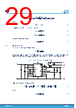
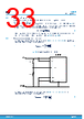
31 / 56 page  9 Application notes 9.1 Output voltage adjustment Primary output voltage The error amplifier reference voltage is 0.85 V typical. The output voltage is adjusted according to the equation below: VOUT_prim=0.85∙1+RFB1RFB2 (22) where RFB1 and RFB2 are the resistors used in the output divider (see figure below). Figure 37. Primary output voltage regulation PGOOD BOOT SW SW VBIAS FB PGND PGND EP GND VOUT_prim VOUT_iso GND_iso L6983I CB RFB1 RFB2 D CSEC COUT A general recommendation is to keep the duty cycle below 50-60%. A higher duty cycle would limit off-time, limiting the time in which the energy transfer to the secondary side takes place. Other restrictions in the duty cycle selection arise due to the minimum on-time (see Section 9.2 Switching frequency), generally summarized by the following equation: D≥DMIN=TONMIN∙fSW (23) Secondary output voltage In the iso-buck converter, the secondary output voltage is not included in the regulation loop. Nevertheless, a good regulation of the secondary output voltage is achieved by relying on the primary output voltage regulation, and the selection of a proper turn ratio of the transformer as well as considering the voltage drops due to the secondary winding resistance and the Schottky diode. That can be summarized by the following equation: VOUT_sec=N∙ [VOUT_prim+IOUT pri ∙ (RDS(onLS+Rwind_pri)]∙ Lm Lm+LLEAK - Rwind_sec∙I OUT_sec-VFD1 (24) Where N is the turn ratio, Rwind_prim and Rwind_sec are the winding resistances of the primary and secondary side respectively, VFD1 is the forward voltage of the Schottky diode, Lm is the magnetizing inductance of the transformer and LLEAK the leakage inductance of the transformer. If no current is drawn from the primary output, equation 24 can be simplified as follows: VOUT_sec=N∙VOUTprim∙ Lm Lm+LLEAK‐Rwind_sec∙IOUT_sec‐VFD1 (25) L6983I Application notes DS14040 - Rev 1 page 31/56 |
|
链接网址 |
| ALLDATASHEET是否为您带来帮助? [ DONATE ] |
关于 Alldatasheet | 广告服务 | 联系我们 | 隐私政策 | 数据表链接 | 链接交换 | 制造商名单 All Rights Reserved©Alldatasheet.com |
| Russian : Alldatasheetru.com | Korean : Alldatasheet.co.kr | Spanish : Alldatasheet.es | French : Alldatasheet.fr | Italian : Alldatasheetit.com Portuguese : Alldatasheetpt.com | Polish : Alldatasheet.pl | Vietnamese : Alldatasheet.vn Indian : Alldatasheet.in | Mexican : Alldatasheet.com.mx | British : Alldatasheet.co.uk | New Zealand : Alldatasheet.co.nz |
|
Family Site : ic2ic.com |
icmetro.com |
 Chinese ▼
 English
 Chinese
 German
 Japanese
 Russian
 Korean
 Spanish
 French
 Italian
 Portuguese
 Polish
 Vietnamese
 Indian
 Mexican
 British
 New Zealand