|
数据搜索系统,热门电子元器件搜索 |
|
|
数据搜索系统,热门电子元器件搜索 |
|
MPZ2012S221A 数据表(PDF) 42 Page - STMicroelectronics |
|
|
|||||||||||||||||||||||||||||
MPZ2012S221A 数据表(HTML) 42 Page - STMicroelectronics |
|
|
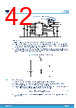
42 / 56 page  Figure 48. RC snubber network VIN VIN VINLDO EN/CLKIN FSW VCC AGND AGND PGOOD BOOT SW SW VBIAS FB PGND PGND EP VIN GND GND VOUT_prim VOUT_iso GND_iso L6983I CIN CLDO RLDO RFSW1 CVCC CB RFB1 RFB2 D CSEC COUT CS RS snubber network Capacitance The parasitic capacitance of a real transformer mainly consists of the following contributions: • Capacitance across each winding (CP and CS, in the image below) due to the capacitive coupling between the coil and the core. As already mentioned, the winding capacitances are involved in the ringing observed during transition from off to on-phase of the primary side. • Interwinding capacitance (CWW), that is the capacitance between windings. The interwinding capacitance should be reduced in order to limit disturbance on the primary side due to possible steep voltage transitions present in the load connected to the secondary output. Figure 49. Transformer parasitic capacitances 10.3 Schottky diode In the selection of the Schottky diode, the following parameters should be considered: • Maximum forward current, mainly defined by the secondary output current demand (see Eq. (44)) • Forward voltage drop, which affects the secondary output voltage regulation • Maximum peak reverse voltage. During the on-phase of the primary side, when in the secondary side no current flows, the diode is reverse biased and must withstand this voltage: VD1_rev=N∙VINmax−VOUT_pri+VOUT_sec (45) • Junction capacitance, which should be as low as possible in order to reduce the ringing described in the previous section L6983I Schottky diode DS14040 - Rev 1 page 42/56 |
|
链接网址 |
| ALLDATASHEET是否为您带来帮助? [ DONATE ] |
关于 Alldatasheet | 广告服务 | 联系我们 | 隐私政策 | 数据表链接 | 链接交换 | 制造商名单 All Rights Reserved©Alldatasheet.com |
| Russian : Alldatasheetru.com | Korean : Alldatasheet.co.kr | Spanish : Alldatasheet.es | French : Alldatasheet.fr | Italian : Alldatasheetit.com Portuguese : Alldatasheetpt.com | Polish : Alldatasheet.pl | Vietnamese : Alldatasheet.vn Indian : Alldatasheet.in | Mexican : Alldatasheet.com.mx | British : Alldatasheet.co.uk | New Zealand : Alldatasheet.co.nz |
|
Family Site : ic2ic.com |
icmetro.com |
 Chinese ▼
 English
 Chinese
 German
 Japanese
 Russian
 Korean
 Spanish
 French
 Italian
 Portuguese
 Polish
 Vietnamese
 Indian
 Mexican
 British
 New Zealand