|
数据搜索系统,热门电子元器件搜索 |
|
|
数据搜索系统,热门电子元器件搜索 |
|
L9963E 数据表(PDF) 7 Page - STMicroelectronics |
|
|
|||||||||||||||||||||||||||||
L9963E 数据表(HTML) 7 Page - STMicroelectronics |
|
|
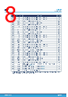
7 / 184 page  Pin # Pin name Description I/O type(1) 5 VCOM Regulated power supply used for communication interfaces. Connect a tank capacitor as indicated in Table 73. Can be used to supply external loads with a maximum IVCOM_ext current budget. P 6 CGND Communication ground. Connect to DGND on top. G 7 ISOHp Non-inverting, high-side isolated serial communication port. Refer to Section 4.2.3 Isolated Serial Peripheral Interface. Refer to Section 6.8 ISO lines circuit. AIO 8 ISOHm Inverting, high-side isolated serial communication port. Refer to Section 4.2.3 Isolated Serial Peripheral Interface. Refer to Section 6.8 ISO lines circuit. AIO 9 DGND Digital ground. Connect to AGND on top. G 10 GPIO1_ FAULTH Digital input used for FAULTH receiver. Refer to Section 4.3 FAULT line. DI 11 GPIO2_ FAULTL Digital output used for FAULTL transmitter. Refer to Section 4.3 FAULT line. DO 12 GPIO3 General-purpose I/O. Refer to Section 4.9 General purpose I/O: GPIOs. Generally used to sense NTCs. Refer to Section 6.9 NTC analog front end. AI/DI/DO 13 GPIO4 AI/DI/DO 14 GPIO5 AI/DI/DO 15 GPIO6 AI/DI/DO 16 GPIO7_ WAKEUP General-purpose I/O. Refer to Section 4.9 General purpose I/O: GPIOs. Generally used to sense NTCs. Refer to Section 6.9 NTC analog front end. Can be configured to act as wake up input. Refer to Section 4.9.4 GPIO7: wake up feature. AI/DI/DO 17 NPNDRV Internal voltage regulator controller output. Connect to the base of the external NPN transistor. AO 18 VREG Regulated analog power supply for core circuitry. Connect a tank capacitor as indicated in Table 73. It is disabled in low power modes (Silent Balancing, Sleep and during the OFF phase of Cyclic Wakeup). VCOM, VANA and VTREF regulators are fed by pre-regulated VREG. P 19 VTREF Buffered, precise analog reference voltage for driving multiple NTCs. Connect a tank capacitor as indicated in Table 73. It has a maximum IVTREF_ext current budget. P 20 SPIEN At first power up, after VCOM is out of undervoltage, this pin is sampled to determine port L configuration. Connect to VCOM to configure SPI mode. Connect to AGND to select isolated SPI communication. If left floating, this pin has a 100KΩ internal Pull down, forcing isolated SPI mode. DI 21 VANA Precise ADC analog supply. Connect a tank capacitor as indicated in Table 73. P 22 AGND Analog/ESD ground. Ground supply of chip. G 23 ISENSEp Non-inverting input of current measurement. Refer to Table 73. AI 24 ISENSEm Inverting input of current measurement. Refer to Table 73. AI 25 GNDREF Analog/reference GND. Connect to AGND on top G 26 C0 Connect to the negative terminal of 1st cell. AI 27 C1 Cell voltage input. Connect to the positive terminal of 1st cell. AI 28 S1 Cell balancing FET control output for 1st cell. AO 29 B2_1 Common terminal for cell balancing S1 and S2. AO 30 S2 Cell balancing FET control output for 2nd cell. AO 31 C2 Cell voltage input. Connect to the positive terminal of 2nd cell. AI 32 C3 Cell voltage input. Connect to the positive terminal of 3rd cell. AI 33 S3 Cell balancing FET control output for 3rd cell. AO 34 B4_3 Common terminal for cell balancing S3 and S4. AO 35 S4 Cell balancing FET control output for 4th cell. AO L9963E Pin description DS13636 - Rev 12 page 7/184 |
|
链接网址 |
| ALLDATASHEET是否为您带来帮助? [ DONATE ] |
关于 Alldatasheet | 广告服务 | 联系我们 | 隐私政策 | 数据表链接 | 链接交换 | 制造商名单 All Rights Reserved©Alldatasheet.com |
| Russian : Alldatasheetru.com | Korean : Alldatasheet.co.kr | Spanish : Alldatasheet.es | French : Alldatasheet.fr | Italian : Alldatasheetit.com Portuguese : Alldatasheetpt.com | Polish : Alldatasheet.pl | Vietnamese : Alldatasheet.vn Indian : Alldatasheet.in | Mexican : Alldatasheet.com.mx | British : Alldatasheet.co.uk | New Zealand : Alldatasheet.co.nz |
|
Family Site : ic2ic.com |
icmetro.com |
 Chinese ▼
 English
 Chinese
 German
 Japanese
 Russian
 Korean
 Spanish
 French
 Italian
 Portuguese
 Polish
 Vietnamese
 Indian
 Mexican
 British
 New Zealand