|
数据搜索系统,热门电子元器件搜索 |
|
|
数据搜索系统,热门电子元器件搜索 |
|
ANT-2.4-CW-RCL-RPS 数据表(PDF) 10 Page - Microchip Technology |
|
|
|||||||||||||||||||||||||||||
ANT-2.4-CW-RCL-RPS 数据表(HTML) 10 Page - Microchip Technology |
|
|
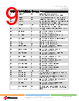
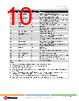
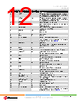
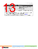
10 / 73 page  WINCS02IC and WINCS02 Family Device Overview Data Sheet © 2024-2025 Microchip Technology Inc. and its subsidiaries DS70005577B - 10 Table 2-1. WINCS02IC Pinout Table (continued) Pin Number Pin Name Pin Type Description 34 DFU_RX/STRAP1 I Device Firmware Update, receive signal Host interface configuration strapping1 pin. Connecting to a pull-up resistor of 10K is recommended. 35 DFU_TX/STRAP2 O Device Firmware Update, transmit signal I Host interface configuration strapping2 pin. Connecting to a pull-up resistor of 10K is recommended. 36 MCLR I Master Clear Reset Input (Active low) 37 AVDD P Input power supply to Analog Block (3.0-3.6V, 3.3V typical) 38 Reserved(7) I/O Reserved pin Connect to an I/O pin (tri-stated) of a host device or to an external switch for future use 39 RTCC_OSC_OUT(5) O 32.768 KHz RTCC oscillator output 40 RTCC_OSC_IN/ PTA_BT_ACTIVE(4)(5) I 32.768 KHz RTCC Oscillator input PTA interface, Bluetooth® Coexistence device active indication input to WINCS02IC 41 VDD33 P Input supply voltage for the Main Power Domain (3.0-3.6V, 3.3V typical) 42 PTA_BT_PRIO I PTA interface, Bluetooth Coexistence device priority indication input to WINCS02IC. 43 PTA_WLAN_ACTIVE O PTA interface, WINCS02IC WLAN active indication output to Bluetooth Coexistence device 44 Reserved I/O Reserved pin Do not connect. 45 VDD33 P Input supply voltage for the Main Power Domain (3.0-3.6V, 3.3V typical) 46 PMU_MLDO_OUT(3) P 1.5V output of on-chip PMU MLDO 47 PMU_VDDP P Input power supply to the on-chip PMU (3.0-3.6V, 3.3V typical) 48 PMU_BK_LX P 1.5V output of on-chip PMU Buck Regulator Connect to an external LC filter (L = 4.7 uH and C = 10 uF) 49 GND P Thermal ground paddle Notes: 1. Refer to the reference design package for exact pin mapping and signal connection. 2. WINCS02IC does not support GPIO functionality. All the pins are reserved. 3. Do not connect any external 1.5V supply. 4. This pin can be used either as an oscillator input pin or as PTA BT_ACTIVE. Both functionalities cannot be supported simultaneously. 5. Current firmware does not support the RTCC oscillator function; it is recommended to have an option to mount the RTCC oscillator in the design to upgrade with the future version of firmware releases. 6. For more details, refer to the WINCS02 Module External Antenna Calibration Guide (DS50003753). 7. Do not leave this pin unconnected. Follow the directions in the Pin Description column for future upgrades. |
|
链接网址 |
| ALLDATASHEET是否为您带来帮助? [ DONATE ] |
关于 Alldatasheet | 广告服务 | 联系我们 | 隐私政策 | 数据表链接 | 链接交换 | 制造商名单 All Rights Reserved©Alldatasheet.com |
| Russian : Alldatasheetru.com | Korean : Alldatasheet.co.kr | Spanish : Alldatasheet.es | French : Alldatasheet.fr | Italian : Alldatasheetit.com Portuguese : Alldatasheetpt.com | Polish : Alldatasheet.pl | Vietnamese : Alldatasheet.vn Indian : Alldatasheet.in | Mexican : Alldatasheet.com.mx | British : Alldatasheet.co.uk | New Zealand : Alldatasheet.co.nz |
|
Family Site : ic2ic.com |
icmetro.com |
 Chinese ▼
 English
 Chinese
 German
 Japanese
 Russian
 Korean
 Spanish
 French
 Italian
 Portuguese
 Polish
 Vietnamese
 Indian
 Mexican
 British
 New Zealand