|
数据搜索系统,热门电子元器件搜索 |
|
|
数据搜索系统,热门电子元器件搜索 |
|
ANT-2.4-CW-RCL-RPS 数据表(PDF) 14 Page - Microchip Technology |
|
|
|||||||||||||||||||||||||||||
ANT-2.4-CW-RCL-RPS 数据表(HTML) 14 Page - Microchip Technology |
|
|
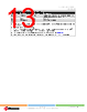
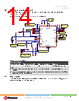
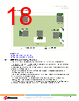
14 / 73 page  WINCS02IC and WINCS02 Family Device Overview Data Sheet © 2024-2025 Microchip Technology Inc. and its subsidiaries DS70005577B - 14 2.3 Basic Connection Requirement The WINCS02 Module requires attention to a minimal set of device pin connections before proceeding with development. Figure 2-4. WINCS02 Module Basic Connection and Interface Diagram 10K DNP R1 100K R2 GND VDD 10K DNP R3 100K R4 GND VDD 10k R7 VDD 0.1uF C4 GND RESET INTOUT PTA_BT_ACTIVE GND PTA_WLAN_ACTIVE PTA_BT_PRIO 1V5 TP1 UART2_TX VDD 0.1uF C2 4.7uF C1 GND GND 0R R11 GND 32.768kHz Y1 GND 18pF C5 18pF C6 0R R9 0R R8 DNP DNP 0R R10 SPI_SDI U1_RX TP3 U1_TX TP2 GND RESET 1 2 3 4 5 6 J1 1x6_Header DFU_RX/STRAP1 DFU_TX/STRAP2 RESET R5 VDD VDD I2C_SCL I2C_SDA I/O UART1_TX UART1_RX SPI_CS SPI_SDO DNP DNP DNP WINCS02_MODULE NC 1 I2C_SCL 2 I2C_SDA 3 MCLR 4 PTA_WLAN_ACTIVE 5 PTA_BT_PRIO 6 RESERVED 7 NC 8 DFU_RX/STRAP1 10 RESERVED 11 INTOUT 13 UART1_TX 14 SDI1 15 CS1 16 SDO1 17 SCK1 18 UART1_RX 19 RTCC_OSC_IN/PTA_BT_ACTIVE 21 RTCC_OSC_OUT 22 TP 24 NC 25 DFU_TX/STRAP2 26 UART2_TX 27 U1 SPI_SCK 5 SW1 0.1uF C3 10k R13 0R R12 VDD GND GND DNP DNP DNP DNP R6 NOTE on UART1: U1_TX and U1_RX will be required for External antenna calibration for some antennas NOTE on DFU: For Device Firmware Update. Add a 2.54mm pitch 1x6 male header to use with a standard USB to UART converter cable for DFU; Otherwise, Add test points only for the 4 required signals NOTE on Strap pins for host interface selection: Strap1: Pulled high for future upgrades Strap2: Pulled high for SPI as a host interface NOTE on UART2: For printing Firmware Debug Logs NOTE on PTA: For coexistance with a Bluetooth Device NOTE on I2C: For communication with Crypto Authentication security device. Placeholder for Pull-ups recommended NOTE on Host Interface: SPI is the host interface NOTE on Supply Pins: 2 supply pins VDD & VDDIO (3 - 3.6V) NOTE on TP Test Point: 1.5V Output from PMU; To confirm internal PMU is working fine NOTE on RTCC OSC: RTCC OSC can be used if coexistance with Bluetooth device is not a requirement for end application NOTE on User Button: Placeholder for User Button recommended for future use Table 2-3. Configuration Details Configuration Details Module Pin10/Strap1 Module Pin26/Strap2(1) Host Interface Selection Description 1 X (Pulled High) SPI WINCS02 Module with SPI Notes: 1. The recommendation is to provide an option to mount the pulled-high resistor in the host board design for future upgrades. 2. The mentioned resistance values are only guidelines. For details on the application schematics, refer to the WINCS02 Add On Board User's Guide (DS50003721). 2.3.1 Power Supply Pin It is recommended to add a bulk and a decoupling capacitor at the input supply Pin 20 (VDD), Pin 23 (VDDIO) and GND of the WINCS02 Module. |
|
链接网址 |
| ALLDATASHEET是否为您带来帮助? [ DONATE ] |
关于 Alldatasheet | 广告服务 | 联系我们 | 隐私政策 | 数据表链接 | 链接交换 | 制造商名单 All Rights Reserved©Alldatasheet.com |
| Russian : Alldatasheetru.com | Korean : Alldatasheet.co.kr | Spanish : Alldatasheet.es | French : Alldatasheet.fr | Italian : Alldatasheetit.com Portuguese : Alldatasheetpt.com | Polish : Alldatasheet.pl | Vietnamese : Alldatasheet.vn Indian : Alldatasheet.in | Mexican : Alldatasheet.com.mx | British : Alldatasheet.co.uk | New Zealand : Alldatasheet.co.nz |
|
Family Site : ic2ic.com |
icmetro.com |
 Chinese ▼
 English
 Chinese
 German
 Japanese
 Russian
 Korean
 Spanish
 French
 Italian
 Portuguese
 Polish
 Vietnamese
 Indian
 Mexican
 British
 New Zealand