|
数据搜索系统,热门电子元器件搜索 |
|
|
数据搜索系统,热门电子元器件搜索 |
|
R5F104FCAFP 数据表(PDF) 47 Page - Renesas Technology Corp |
|
|
|||||||||||||||||||||||||||||
R5F104FCAFP 数据表(HTML) 47 Page - Renesas Technology Corp |
|
|
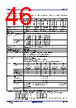
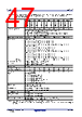
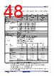
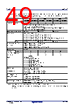
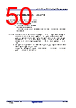
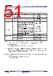
47 / 207 page  RL78/G13 1. OUTLINE R01DS0131EJ0350 Rev.3.50 47 of 200 Jun 30, 2020 Notes 2. The number of PWM outputs varies depending on the setting of channels in use (the number of masters and slaves) (see 6.9.3 Operation as multiple PWM output function in the RL78/G13 User’s Manual). 3. When setting to PIOR = 1 (2/2) Item 40-pin 44-pin 48-pin 52-pin 64-pin Clock output/buzzer output 2 2 2 2 2 ● 2.44 kHz, 4.88 kHz, 9.76 kHz, 1.25 MHz, 2.5 MHz, 5 MHz, 10 MHz (Main system clock: fMAIN = 20 MHz operation) ● 256 Hz, 512 Hz, 1.024 kHz, 2.048 kHz, 4.096 kHz, 8.192 kHz, 16.384 kHz, 32.768 kHz (Subsystem clock: fSUB = 32.768 kHz operation) 8/10-bit resolution A/D converter 9 channels 10 channels 10 channels 12 channels 12 channels Serial interface [40-pin, 44-pin products] ● CSI: 1 channel/simplified I2C: 1 channel/UART: 1 channel ● CSI: 1 channel/simplified I2C: 1 channel/UART: 1 channel ● CSI: 2 channels/simplified I2C: 2 channels/UART (UART supporting LIN-bus): 1 channel [48-pin, 52-pin products] ● CSI: 2 channels/simplified I2C: 2 channels/UART: 1 channel ● CSI: 1 channel/simplified I2C: 1 channel/UART: 1 channel ● CSI: 2 channels/simplified I2C: 2 channels/UART (UART supporting LIN-bus): 1 channel [64-pin products] ● CSI: 2 channels/simplified I2C: 2 channels/UART: 1 channel ● CSI: 2 channels/simplified I2C: 2 channels/UART: 1 channel ● CSI: 2 channels/simplified I2C: 2 channels/UART (UART supporting LIN-bus): 1 channel I2C bus 1 channel 1 channel 1 channel 1 channel 1 channel Multiplier and divider/multiply- accumulator ● 16 bits × 16 bits = 32 bits (Unsigned or signed) ● 32 bits ÷ 32 bits = 32 bits (Unsigned) ● 16 bits × 16 bits + 32 bits = 32 bits (Unsigned or signed) DMA controller 2 channels Vectored interrupt sources Internal 27 27 27 27 27 External 7 7 10 12 13 Key interrupt 4 4 6 8 8 Reset ● Reset by RESET pin ● Internal reset by watchdog timer ● Internal reset by power-on-reset ● Internal reset by voltage detector ● Internal reset by illegal instruction execution Note ● Internal reset by RAM parity error ● Internal reset by illegal-memory access Power-on-reset circuit ● Power-on-reset: 1.51 V (TYP.) ● Power-down-reset:1.50 V (TYP.) Voltage detector ● Rising edge : 1.67 V to 4.06 V (14 stages) ● Falling edge : 1.63 V to 3.98 V (14 stages) On-chip debug function Provided Power supply voltage VDD = 1.6 to 5.5 V (TA = -40 to +85°C) VDD = 2.4 to 5.5 V (TA = -40 to +105°C) Operating ambient temperature TA = 40 to +85°C (A: Consumer applications, D: Industrial applications) TA = 40 to +105°C (G: Industrial applications) Note The illegal instruction is generated when instruction code FFH is executed. Reset by the illegal instruction execution not issued by emulation with the in-circuit emulator or on-chip debug emulator. |
|
链接网址 |
| ALLDATASHEET是否为您带来帮助? [ DONATE ] |
关于 Alldatasheet | 广告服务 | 联系我们 | 隐私政策 | 数据表链接 | 链接交换 | 制造商名单 All Rights Reserved©Alldatasheet.com |
| Russian : Alldatasheetru.com | Korean : Alldatasheet.co.kr | Spanish : Alldatasheet.es | French : Alldatasheet.fr | Italian : Alldatasheetit.com Portuguese : Alldatasheetpt.com | Polish : Alldatasheet.pl | Vietnamese : Alldatasheet.vn Indian : Alldatasheet.in | Mexican : Alldatasheet.com.mx | British : Alldatasheet.co.uk | New Zealand : Alldatasheet.co.nz |
|
Family Site : ic2ic.com |
icmetro.com |
 Chinese ▼
 English
 Chinese
 German
 Japanese
 Russian
 Korean
 Spanish
 French
 Italian
 Portuguese
 Polish
 Vietnamese
 Indian
 Mexican
 British
 New Zealand