|
数据搜索系统,热门电子元器件搜索 |
|
|
数据搜索系统,热门电子元器件搜索 |
|
R5F104FCAFP 数据表(PDF) 24 Page - Renesas Technology Corp |
|
|
|||||||||||||||||||||||||||||
R5F104FCAFP 数据表(HTML) 24 Page - Renesas Technology Corp |
|
|
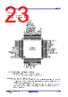
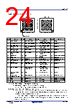
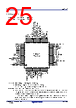
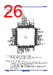
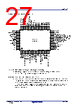
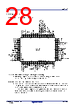
24 / 207 page  RL78/G13 1. OUTLINE R01DS0131EJ0350 Rev.3.50 24 of 200 Jun 30, 2020 ● 64-pin plastic VFBGA (4 × 4 mm, 0.4-mm pitch) 1 HGF E D C B A 2 3 4 5 6 7 8 RL78/G13 (Top View) AB C D E F G H Top View Bottom View Index mark Pin No. Name Pin No. Name Pin No. Name Pin No. Name A1 P05/TI05/TO05 C1 P51/INTP2/SO11 E1 P13/TxD2/SO20/ (SDAA0)/(TI04)/(TO04) G1 P146 A2 P30/INTP3/RTC1HZ /SCK11/SCL11 C2 P71/KR1/SI21/SDA21 E2 P14/RxD2/SI20/SDA20 /(SCLA0)/(TI03)/(TO03) G2 P25/ANI5 A3 P70/KR0/SCK21 /SCL21 C3 P74/KR4/INTP8/SI01 /SDA01 E3 P15/SCK20/SCL20/ (TI02)/(TO02) G3 P24/ANI4 A4 P75/KR5/INTP9 /SCK01/SCL01 C4 P52/(INTP10) E4 P16/TI01/TO01/INTP5 /(SI00)/(RxD0) G4 P22/ANI2 A5 P77/KR7/INTP11/ (TxD2) C5 P53/(INTP11) E5 P03/ANI16/SI10/RxD1 /SDA10 G5 P130 A6 P61/SDAA0 C6 P63 E6 P41/TI07/TO07 G6 P02/ANI17/SO10/TxD1 A7 P60/SCLA0 C7 VSS E7 RESET G7 P00/TI00 A8 EVDD0 C8 P121/X1 E8 P137/INTP0 G8 P124/XT2/EXCLKS B1 P50/INTP1/SI11 /SDA11 D1 P55/(PCLBUZ1)/ (SCK00) F1 P10/SCK00/SCL00/ (TI07)/(TO07) H1 P147/ANI18 B2 P72/KR2/SO21 D2 P06/TI06/TO06 F2 P11/SI00/RxD0 /TOOLRxD/SDA00/ (TI06)/(TO06) H2 P27/ANI7 B3 P73/KR3/SO01 D3 P17/TI02/TO02/ (SO00)/(TxD0) F3 P12/SO00/TxD0 /TOOLTxD/(INTP5)/ (TI05)/(TO05) H3 P26/ANI6 B4 P76/KR6/INTP10/ (RxD2) D4 P54 F4 P21/ANI1/AVREFM H4 P23/ANI3 B5 P31/TI03/TO03 /INTP4/(PCLBUZ0) D5 P42/TI04/TO04 F5 P04/SCK10/SCL10 H5 P20/ANI0/AVREFP B6 P62 D6 P40/TOOL0 F6 P43 H6 P141/PCLBUZ1/INTP7 B7 VDD D7 REGC F7 P01/TO00 H7 P140/PCLBUZ0/INTP6 B8 EVSS0 D8 P122/X2/EXCLK F8 P123/XT1 H8 P120/ANI19 Cautions 1. Make EVSS0 pin the same potential as VSS pin. 2. Make VDD pin the potential that is no less than EVDD0 pin. 3. Connect the REGC pin to Vss via a capacitor (0.47 to 1 µF). Remarks 1. For pin identification, see 1.4 Pin Identification. 2. When using the microcontroller for an application where the noise generated inside the microcontroller must be reduced, it is recommended to supply separate powers to the VDD and EVDD0 pins and connect the VSS and EVSS0 pins to separate ground lines. 3. Functions in parentheses in the above figure can be assigned via settings in the peripheral I/O redirection register (PIOR). Refer to Figure 4-8 Format of Peripheral I/O Redirection Register (PIOR) in the RL78/G13 User’s Manual. |
|
链接网址 |
| ALLDATASHEET是否为您带来帮助? [ DONATE ] |
关于 Alldatasheet | 广告服务 | 联系我们 | 隐私政策 | 数据表链接 | 链接交换 | 制造商名单 All Rights Reserved©Alldatasheet.com |
| Russian : Alldatasheetru.com | Korean : Alldatasheet.co.kr | Spanish : Alldatasheet.es | French : Alldatasheet.fr | Italian : Alldatasheetit.com Portuguese : Alldatasheetpt.com | Polish : Alldatasheet.pl | Vietnamese : Alldatasheet.vn Indian : Alldatasheet.in | Mexican : Alldatasheet.com.mx | British : Alldatasheet.co.uk | New Zealand : Alldatasheet.co.nz |
|
Family Site : ic2ic.com |
icmetro.com |
 Chinese ▼
 English
 Chinese
 German
 Japanese
 Russian
 Korean
 Spanish
 French
 Italian
 Portuguese
 Polish
 Vietnamese
 Indian
 Mexican
 British
 New Zealand