|
数据搜索系统,热门电子元器件搜索 |
|
|
数据搜索系统,热门电子元器件搜索 |
|
R5F104FCAFP 数据表(PDF) 89 Page - Renesas Technology Corp |
|
|
|||||||||||||||||||||||||||||
R5F104FCAFP 数据表(HTML) 89 Page - Renesas Technology Corp |
|
|
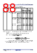
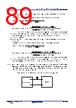
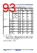
89 / 207 page  RL78/G13 2. ELECTRICAL SPECIFICATIONS (TA = –40 to +85°C) R01DS0131EJ0350 Rev.3.50 89 of 200 Jun 30, 2020 Notes 3. The smaller maximum transfer rate derived by using fMCK/6 or the following expression is the valid maximum transfer rate. Expression for calculating the transfer rate when 2.7 V ≤ EVDD0 < 4.0 V and 2.3 V ≤ Vb ≤ 2.7 V Maximum transfer rate = 1 [bps] {–Cb × Rb × ln (1 – 2.0 Vb )} × 3 1 Transfer rate × 2 – {–Cb × Rb × ln (1 – 2.0 Vb )} Baud rate error (theoretical value) = × 100 [%] ( 1 Transfer rate ) × Number of transferred bits * This value is the theoretical value of the relative difference between the transmission and reception sides. 4. This value as an example is calculated when the conditions described in the “Conditions” column are met. Refer to Note 3 above to calculate the maximum transfer rate under conditions of the customer. 5. Use it with EVDD0 ≥ Vb. 6. The smaller maximum transfer rate derived by using fMCK/6 or the following expression is the valid maximum transfer rate. Expression for calculating the transfer rate when 1.8 V ≤ EVDD0 < 3.3 V and 1.6 V ≤ Vb ≤ 2.0 V Maximum transfer rate = 1 [bps] {–Cb × Rb × ln (1 – 1.5 Vb )} × 3 1 Transfer rate × 2 – {–Cb × Rb × ln (1 – 1.5 Vb )} Baud rate error (theoretical value) = × 100 [%] ( 1 Transfer rate ) × Number of transferred bits * This value is the theoretical value of the relative difference between the transmission and reception sides. 7. This value as an example is calculated when the conditions described in the “Conditions” column are met. Refer to Note 6 above to calculate the maximum transfer rate under conditions of the customer. Caution Select the TTL input buffer for the RxDq pin and the N-ch open drain output (VDD tolerance (When 20- to 52-pin products)/EVDD tolerance (When 64- to 128-pin products)) mode for the TxDq pin by using port input mode register g (PIMg) and port output mode register g (POMg). For VIH and VIL, see the DC characteristics with TTL input buffer selected. UART mode connection diagram (during communication at different potential) RL78 microcontroller TxDq RxDq User device Rx Tx Vb Rb |
|
链接网址 |
| ALLDATASHEET是否为您带来帮助? [ DONATE ] |
关于 Alldatasheet | 广告服务 | 联系我们 | 隐私政策 | 数据表链接 | 链接交换 | 制造商名单 All Rights Reserved©Alldatasheet.com |
| Russian : Alldatasheetru.com | Korean : Alldatasheet.co.kr | Spanish : Alldatasheet.es | French : Alldatasheet.fr | Italian : Alldatasheetit.com Portuguese : Alldatasheetpt.com | Polish : Alldatasheet.pl | Vietnamese : Alldatasheet.vn Indian : Alldatasheet.in | Mexican : Alldatasheet.com.mx | British : Alldatasheet.co.uk | New Zealand : Alldatasheet.co.nz |
|
Family Site : ic2ic.com |
icmetro.com |
 Chinese ▼
 English
 Chinese
 German
 Japanese
 Russian
 Korean
 Spanish
 French
 Italian
 Portuguese
 Polish
 Vietnamese
 Indian
 Mexican
 British
 New Zealand