|
数据搜索系统,热门电子元器件搜索 |
|
|
数据搜索系统,热门电子元器件搜索 |
|
MPC5553 数据表(PDF) 22 Page - Freescale Semiconductor, Inc |
|
|
|||||||||||||||||||||||||||||
MPC5553 数据表(HTML) 22 Page - Freescale Semiconductor, Inc |
|
|
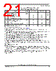
22 / 66 page  MPC5553 Microcontroller Data Sheet, Rev. 2.0 Electrical Characteristics Freescale Semiconductor 22 3.10 eQADC Electrical Characteristics Table 13. eQADC Conversion Specifications (Operating) Spec Characteristic Symbol Minimum Maximum Unit 1 ADC clock (ADCLK) frequency1 1 Conversion characteristics vary with F ADCLK rate. Reduced conversion accuracy occurs at maximum FADCLK rate. The maximum value is based on 800 KS/s and the minimum value is based on 20 MHz oscillator clock frequency divided by a maximum 16 factor. FADCLK 112 MHz 2 Conversion cycles Differential Single ended CC 13 + 2 (15) 14 + 2 (16) 13 + 128 (141) 14 + 128 (142) ADCLK cycles 3 Stop mode recovery time2 2 Stop mode recovery time begins when the ADC control register enable bits are set until the ADC is ready to perform conversions. TSR 10 — μs 4 Resolution3 3 At V RH – VRL = 5.12 V, one least significant bit (LSB) = 1.25, mV = one count. —1.25 — mV 5 INL: 6 MHz ADC clock INL6 –4 4 Counts3 6 INL: 12 MHz ADC clock INL12 –8 8 Counts 7 DNL: 6 MHz ADC clock DNL6 –3 4 4 Guaranteed 10-bit monotonicity. 3 4 Counts 8 DNL: 12 MHz ADC clock DNL12 –6 4 64 Counts 9 Offset error with calibration OFFWC –4 5 5 The absolute value of the offset error without calibration ≤ 100 counts. 4 5 Counts 10 Full-scale gain error with calibration GAINWC –8 6 6 The absolute value of the full scale gain error without calibration ≤ 120 counts. 8 6 Counts 11 Disruptive input injection current 7, 8, 9, 10 7 Below disruptive current conditions, the channel being stressed has conversion values of: 0x3FF for analog inputs greater than VRH, and 0x000 for values less than VRL. This assumes that VRH ≤ VDDA and VRL ≥ VSSA due to the presence of the sample amplifier. Other channels are not affected by non-disruptive conditions. 8 Exceeding the limit can cause a conversion error on both stressed and unstressed channels. Transitions within the limit do not affect device reliability or cause permanent damage. 9 Input must be current limited to the value specified. To determine the value of the required current-limiting resistor, calculate resistance values using VPOSCLAMP = VDDA + 0.5 V and VNEGCLAMP = – 0.3 V, then use the larger of the calculated values. 10 Condition applies to two adjacent pads on the internal pad. IINJ –1 1 mA 12 Incremental error due to injection current. All channels have same 10 k Ω < Rs <100 kΩ Channel under test has Rs = 10 k Ω, IINJ = IINJMAX, IINJMIN EINJ –4 4 Counts 13 Total Unadjusted Error for single ended conversions with calibration11, 12, 13, 14, 15 11 The TUE specification is always less than the sum of the INL, DNL, offset, and gain errors due to canceling errors. 12 TUE does not apply to differential conversions. 13 Measured at 6 MHz ADC clock. TUE with a 12 MHz ADC clock is: –16 counts < TUE < 16 counts. 14 TUE includes all internal device errors such as internal reference variation (75% Ref, 25% Ref). 15 Depending on the input impedance, the analog input leakage current (DC Electrical specification 35a) can affect the actual TUE measured on analog channels AN[12], AN[13], AN[14], AN[15]. TUE –4 4 Counts |
|
链接网址 |
| ALLDATASHEET是否为您带来帮助? [ DONATE ] |
关于 Alldatasheet | 广告服务 | 联系我们 | 隐私政策 | 数据表链接 | 链接交换 | 制造商名单 All Rights Reserved©Alldatasheet.com |
| Russian : Alldatasheetru.com | Korean : Alldatasheet.co.kr | Spanish : Alldatasheet.es | French : Alldatasheet.fr | Italian : Alldatasheetit.com Portuguese : Alldatasheetpt.com | Polish : Alldatasheet.pl | Vietnamese : Alldatasheet.vn Indian : Alldatasheet.in | Mexican : Alldatasheet.com.mx | British : Alldatasheet.co.uk | New Zealand : Alldatasheet.co.nz |
|
Family Site : ic2ic.com |
icmetro.com |
 Chinese ▼
 English
 Chinese
 German
 Japanese
 Russian
 Korean
 Spanish
 French
 Italian
 Portuguese
 Polish
 Vietnamese
 Indian
 Mexican
 British
 New Zealand