|
数据搜索系统,热门电子元器件搜索 |
|
|
数据搜索系统,热门电子元器件搜索 |
|
MPC5553 数据表(PDF) 5 Page - Freescale Semiconductor, Inc |
|
|
|||||||||||||||||||||||||||||
MPC5553 数据表(HTML) 5 Page - Freescale Semiconductor, Inc |
|
|
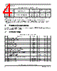
5 / 66 page  Electrical Characteristics MPC5553 Microcontroller Data Sheet, Rev. 2.0 Freescale Semiconductor 5 17 VRH to VDDA differential voltage VRH – VDDA –5.5 5.5 V 18 VRL to VSSA differential voltage VRL – VSSA –0.3 0.3 V 19 VDDEH to VDDA differential voltage VDDEH – VDDA –VDDA VDDEH V 20 VDDF to VDD differential voltage VDDF – VDD –0.3 0.3 V 21 This spec has been moved to Table 9, spec 43a. 22 VSSSYN to VSS differential voltage VSSSYN – VSS –0.1 0.1 V 23 VRCVSS to VSS differential voltage VRCVSS – VSS –0.1 0.1 V 24 Maximum DC digital input current 9 (per pin, applies to all digital pins) 5 IMAXD –2 2 mA 25 Maximum DC analog input current 10 (per pin, applies to all analog pins) IMAXA –3 3 mA 26 Maximum operating temperature range 11 Die junction temperature TJ TL 150.0 oC 27 Storage temperature range TSTG –55.0 150.0 oC 28 Maximum solder temperature 12 TSDR — 260.0 oC 29 Moisture sensitivity level 13 MSL — 3 1 Functional operating conditions are given in the DC electrical specifications. Absolute maximum ratings are stress ratings only, and functional operation at the maxima is not guaranteed. Stress beyond the listed maxima can affect device reliability or cause permanent damage to the device. 2 Absolute maximum voltages are currently maximum burn-in voltages. Absolute maximum specifications for device stress have not yet been determined. 3 1.5 V +/– 10% for proper operation. This parameter is specified at a maximum junction temperature of 150 oC. 4 All functional non-supply I/O pins are clamped to V SS and VDDE, or VDDEH. 5 AC signal overshoot and undershoot of up to +/– 2.0 V of the input voltages is permitted for an accumulative duration of 60 hours over the complete lifetime of the device (injection current not limited for this duration). 6 Internal structures hold the voltage greater than –1.0 V if the injection current limit of 2 mA is met. Keep the negative DC current greater than –0.6 V on eTPUB[15] and SINB during the internal power-on reset (POR) state. 7 Internal structures hold the input voltage less than the maximum voltage on all pads powered by V DDEH supplies, if the maximum injection current specification is met (2 mA for all pins) and VDDEH is within the operating voltage specifications. 8 Internal structures hold the input voltage less than the maximum voltage on all pads powered by V DDE supplies, if the maximum injection current specification is met (2 mA for all pins) and VDDE is within the operating voltage specifications. 9 Total injection current for all pins (including both digital and analog) must not exceed 25 mA. 10 Total injection current for all analog input pins must not exceed 15 mA. 11 Lifetime operation at these specification limits is not guaranteed. 12 Solder profile per CDF-AEC-Q100. 13 Moisture sensitivity per JEDEC test method A112. Table 2. Absolute Maximum Ratings1 (continued) Spec Characteristic Symbol Min Max2 Unit |
|
链接网址 |
| ALLDATASHEET是否为您带来帮助? [ DONATE ] |
关于 Alldatasheet | 广告服务 | 联系我们 | 隐私政策 | 数据表链接 | 链接交换 | 制造商名单 All Rights Reserved©Alldatasheet.com |
| Russian : Alldatasheetru.com | Korean : Alldatasheet.co.kr | Spanish : Alldatasheet.es | French : Alldatasheet.fr | Italian : Alldatasheetit.com Portuguese : Alldatasheetpt.com | Polish : Alldatasheet.pl | Vietnamese : Alldatasheet.vn Indian : Alldatasheet.in | Mexican : Alldatasheet.com.mx | British : Alldatasheet.co.uk | New Zealand : Alldatasheet.co.nz |
|
Family Site : ic2ic.com |
icmetro.com |
 Chinese ▼
 English
 Chinese
 German
 Japanese
 Russian
 Korean
 Spanish
 French
 Italian
 Portuguese
 Polish
 Vietnamese
 Indian
 Mexican
 British
 New Zealand