|
数据搜索系统,热门电子元器件搜索 |
|
|
数据搜索系统,热门电子元器件搜索 |
|
AD9142ABCPZ 数据表(PDF) 39 Page - Analog Devices |
|
|
|||||||||||||||||||||||||||||
AD9142ABCPZ 数据表(HTML) 39 Page - Analog Devices |
|
|
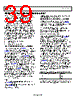
39 / 73 page  AD9142A Data Sheet MULTIDEVICE SYNCHRONIZATION AND FIXED LATENCY A DAC introduces a variation of pipeline latency to a system. The latency variation causes the phase of a DAC output to vary from power-on to power-on. Therefore, the output from different DAC devices may not be perfectly aligned even with well aligned clocks and digital inputs. The skew between multiple DAC outputs varies from power-on to power-on. In applications such as transmit diversity or digital predistortion, where deterministic latency is desired, the variation of the pipeline latency must be minimized. Deterministic latency in this data sheet is defined as a fixed time delay from the digital input to the analog output in a DAC from power-on to power-on. Multiple DAC devices are considered synchronized to each other when each DAC in this group has the same constant latency from power-on to power-on. Three conditions must be identical in all of the ready-to-sync devices before these devices are considered synchronized: • The phase of DAC internal clocks • The FIFO level • The alignment of the input data VERY SMALL INHERENT LATENCY VARIATION The innovative architecture of the AD9142A minimizes the inherent latency variation. The worst-case variation in the AD9142A is two DAC clock cycles. For example, in the case of a 1.5 GHz sample rate, the variation is less than 1.4 ns in any scenario. Therefore, without turning on the synchronization engine, the DAC outputs from multiple AD9142A devices are guaranteed to be aligned within two DAC clock cycles, regardless of the timing between the DCI and the DACCLK. No additional clocks are required to achieve this accuracy. The user must reset the FIFO in each DAC device through the SPI at startup. Therefore, the AD9142A can decrease the complexity of system design in multitransmit channel applications. Note the alignment of the DCI signals in the design. The DCI is used as a reference in the AD9142A design to align the FIFO and the phase of internal clocks in multiple devices. The achieved DAC output alignment depends on how well the DCI signals are aligned at the input of each device. The following equation is the expression of the worst-case DAC output alignment accuracy in the case of DCI signal mismatches. tSK (OUT) = tSK (DCI) + 2/fDAC where: tSK (OUT) is the worst-case skew between the DAC output from two AD9142A devices. tSK (DCI) is the skew between two DCI signals at the DCI input of the two AD9142A devices. fDAC is the DACCLK frequency. The better the alignment of the DCI signals, the smaller is the overall skew between two DAC outputs. FURTHER REDUCING THE LATENCY VARIATION For applications that require finer synchronization accuracy (DAC latency variation < 2 DAC clock cycles), the AD9142A has a provision for enabling multiple devices to be synchronized to each other within a single DAC clock cycle. To further reduce the latency variation in the DAC, the synchronization machine needs to be turned on and two external clocks (frame and sync) need to be generated in the system and fed to all the DAC devices. Set Up and Hold Timing Requirement The sync clock (fSYNC) serves as a reference clock in the system to reset the clock generation circuitry in multiple AD9142A devices simultaneously. Inside the DAC, the sync clock is sampled by the DACCLK to generate a reference point for aligning the internal clocks, so there is a setup and hold timing requirement between the sync clock and the DAC clock. If the user adopts the continuous frame reset mode, that is, the FIFO and sync engine periodically reset, the timing requirements between the sync clock and the DAC clock must be met. Otherwise, the device can lose lock and corrupt the output. In the one shot frame reset mode, it is still recommended that this timing be met at the time when the sync routine is run because not meeting the timing can degrade the sync alignment accuracy by one DAC cycle, as shown in Table 22. For users who want to synchronize the device in a one-shot manner and continue to monitor the synchronization status, the AD9142A provides a sync monitoring mode. It provides a continuous sync and frame clock to synchronize the part once and ignore the clock cycles after the first valid frame pulse is detected. In this way, the user can monitor the sync status without periodically resynchronizing the device; to engage the sync monitoring mode, set Register 0x22[1:0] (FRAME_RESET_ MODE) to 11b. Table 22. Sync Clock and DAC Clock Setup and Hold Times Falling Edge Sync Timing (default) Max (ps) tS (ns) 324 tH (ns)1 −92 |tS + tH| (ns) 232 1 The negative sign indicates the direction of the setup time. The setup time is defined as positive when it is on the left side of the clock edge and negative when it is on the right side of the clock edge. Rev. A | Page 38 of 72 |
|
链接网址 |
| ALLDATASHEET是否为您带来帮助? [ DONATE ] |
关于 Alldatasheet | 广告服务 | 联系我们 | 隐私政策 | 数据表链接 | 链接交换 | 制造商名单 All Rights Reserved©Alldatasheet.com |
| Russian : Alldatasheetru.com | Korean : Alldatasheet.co.kr | Spanish : Alldatasheet.es | French : Alldatasheet.fr | Italian : Alldatasheetit.com Portuguese : Alldatasheetpt.com | Polish : Alldatasheet.pl | Vietnamese : Alldatasheet.vn Indian : Alldatasheet.in | Mexican : Alldatasheet.com.mx | British : Alldatasheet.co.uk | New Zealand : Alldatasheet.co.nz |
|
Family Site : ic2ic.com |
icmetro.com |
 Chinese ▼
 English
 Chinese
 German
 Japanese
 Russian
 Korean
 Spanish
 French
 Italian
 Portuguese
 Polish
 Vietnamese
 Indian
 Mexican
 British
 New Zealand