|
数据搜索系统,热门电子元器件搜索 |
|
|
数据搜索系统,热门电子元器件搜索 |
|
AD9142ABCPZ 数据表(PDF) 68 Page - Analog Devices |
|
|
|||||||||||||||||||||||||||||
AD9142ABCPZ 数据表(HTML) 68 Page - Analog Devices |
|
|
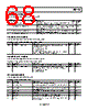
68 / 73 page  Data Sheet AD9142A DAC OUTPUT CONTROL REGISTER Address: 0x44, Reset: 0x8D, Name: DAC_OUTPUT_CTRL Table 88. Bit Descriptions for DAC_OUTPUT_CTRL Bits Bit Name Settings Description Reset Access 7 DAC_OUTPUT_CTRL_EN Enables the DAC output control. This bit needs to be set to 1 to enable the remaining bits in this register. 0x1 RW 3 FIFO_WARNING_SHUTDOWN_EN When this bit and Bit 7 are both high, if a FIFO warning occurs, the DAC output shuts down automatically. By default, this function is on. 0x1 RW 2 OVERTHRESHOLD_SHUTDOWN_EN The DAC output is turned off when the input average power is greater than the predefined threshold. 0x1 RW 0 FIFO_ERROR_SHUTDOWN_EN The DAC output is turned off when the FIFO reports warnings. 0x1 RW DLL CELL ENABLE 0 REGISTER Address: 0x5E, Reset: 0xFF, Name: ENABLE_DLL_DELAY_CELL0 Table 89. Bit Descriptions for ENABLE_DLL_DELAY_CELL0 Bits Bit Name Description Reset Access [7:0] DELAY_CELL_ENABLE [7:0] Set each bit to enable or disable the delay cell. Delay cell number corresponds to bit number. 0xFF RW 1 = enable delay cell (default). 0 = disable delay cell. Different recommended values should be used in DLL mode and delay line mode. See the Data Interface section. DLL CELL ENABLE 1 REGISTER Address: 0x5F, Reset: 0x67, Name: ENABLE_DLL_DELAY_CELL1 Table 90. Bit Descriptions for ENABLE_DLL_DELAY_CELL1 Bits Bit Name Description Reset Access [7:3] Reserved Must write the default value for optimal performance. 0x0C RW [2:0] DELAY_CELL_ENABLE [10:8] Set each bit to enable or disable the delay cell. Delay cell numbers are 10, 9, 8 corresponding to bits Bit, Bit 2, and Bit 0, respectively. 0x7 RW 1 = enable delay cell (default). 0 = disable delay cell. SED CONTROL REGISTER Address: 0x60, Reset: 0x00, Name: SED_CTRL Table 91. Bit Descriptions for SED_CTRL Bits Bit Name Description Reset Access 7 SED_ENABLE Set to 1 to Enable the SED compare logic. 0 RW 6 SED_ERR_CLEAR When set to 1, clears all SED reported error bits, Bit 2, Bit 1, and Bit 0. 0 RW 5 AED_ENABLE When set to 1, enables the AED function (SED with auto clear after eight passing sets). 0 RW 4 SED_DEPTH 0 = SED depth of two words, 1 = SED depth of four words. 0 RW 3 Reserved Reserved. 0 R 2 AED_PASS When AED = 1, it signals eight true compare cycles. 0 RW 1 AED_FAIL When AED = 1, it signals a mismatch in comparison. 0 R 0 SED_FAIL Signals that an SED mismatch in comparison occurred (with SED or AED enabled). 0 R Rev. A | Page 67 of 72 |
|
链接网址 |
| ALLDATASHEET是否为您带来帮助? [ DONATE ] |
关于 Alldatasheet | 广告服务 | 联系我们 | 隐私政策 | 数据表链接 | 链接交换 | 制造商名单 All Rights Reserved©Alldatasheet.com |
| Russian : Alldatasheetru.com | Korean : Alldatasheet.co.kr | Spanish : Alldatasheet.es | French : Alldatasheet.fr | Italian : Alldatasheetit.com Portuguese : Alldatasheetpt.com | Polish : Alldatasheet.pl | Vietnamese : Alldatasheet.vn Indian : Alldatasheet.in | Mexican : Alldatasheet.com.mx | British : Alldatasheet.co.uk | New Zealand : Alldatasheet.co.nz |
|
Family Site : ic2ic.com |
icmetro.com |
 Chinese ▼
 English
 Chinese
 German
 Japanese
 Russian
 Korean
 Spanish
 French
 Italian
 Portuguese
 Polish
 Vietnamese
 Indian
 Mexican
 British
 New Zealand