|
数据搜索系统,热门电子元器件搜索 |
|
|
数据搜索系统,热门电子元器件搜索 |
|
AD9142ABCPZ 数据表(PDF) 45 Page - Analog Devices |
|
|
|||||||||||||||||||||||||||||
AD9142ABCPZ 数据表(HTML) 45 Page - Analog Devices |
|
|
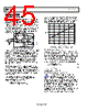
45 / 73 page  AD9142A Data Sheet Rev. A | Page 44 of 72 ANALOG OUTPUTS TRANSMIT DAC OPERATION Figure 56 shows a simplified block diagram of the transmit path DACs. The DAC core consists of a current source array, a switch core, digital control logic, and full-scale output current control. The DAC full-scale output current (IOUTFS) is nominally 20 mA. The output currents from the IOUT1P/IOUT2P and IOUT1N/ IOUT2N pins are complementary, meaning that the sum of the two currents always equals the full-scale current of the DAC. The digital input code to the DAC determines the effective differential current delivered to the load. Figure 56. Simplified Block Diagram of DAC Core The DAC has a 1.2 V band gap reference with an output imped- ance of 5 kΩ. The reference output voltage appears on the VREF pin. When using the internal reference, decouple the VREF pin to AVSS with a 0.1 μF capacitor. Use the internal reference only for external circuits that draw dc currents of 2 μA or less. For dynamic loads or static loads greater than 2 μA, buffer the VREF pin. If desired, the internal reference can be overdriven by applying an external reference (from 1.10 V to 1.30 V) to the VREF pin. A 10 kΩ external resistor, RSET, must be connected from the FSADJ pin to AVSS. This resistor, together with the reference control amplifier, sets up the correct internal bias currents for the DAC. Because the full-scale current is inversely proportional to this resistor, the tolerance of RSET is reflected in the full-scale output amplitude. The full-scale current equation, where the DAC gain is individually set for the Q and I DACs in Register 0x40 and Register 0x44, respectively, is as follows: DAC gain R V I SET REF FS 16 3 72 For nominal values of VREF (1.2 V), RSET (10 kΩ), and DAC gain (512), the full-scale current of the DAC is typically 20 mA. The DAC full-scale current can be adjusted from 8.64 mA to 31.68 mA by setting the DAC gain parameter, as shown in Figure 57. Figure 57. DAC Full-Scale Current vs. DAC Gain Code Transmit DAC Transfer Function The output currents from the IOUT1P/IOUT2P and IOUT1N/ IOUT2N pins are complementary, meaning that the sum of the two currents always equals the full-scale current of the DAC. The digital input code to the DAC determines the effective differen- tial current delivered to the load. IOUT1P/IOUT2P provide maximum output current when all bits are high. The output currents vs. DACCODE for the DAC outputs is expressed as OUTFS N OUTP I DACCODE I 2 (1) IOUTN = IOUTFS – IOUTP (2) where DACCODE = 0 to 2N − 1. Transmit DAC Output Configurations The optimum noise and distortion performance of the AD9142A is realized when it is configured for differential operation. The common-mode rejection of a transformer or differential amplifier significantly reduces the common-mode error sources of the DAC outputs. These common-mode error sources include even-order distortion products and noise. The enhancement in distortion performance becomes more significant as the frequency content of the reconstructed waveform increases and/or its amplitude increases. This is due to the first- order cancellation of various dynamic common-mode distortion mechanisms, digital feedthrough, and noise. I DAC IOUT1P IOUT1N Q DAC IOUT2N IOUT2P CURRENT SCALING I DAC FS ADJUST REG 0x18, REG 0x19 Q DAC FS ADJUST REG 0x1A, REG 0x1B 0.1µF 10kΩ RSET FSADJ VREF 5kΩ 1.2V 35 0 01000 DAC GAIN CODE 30 25 20 15 10 5 200 400 600 800 |
|
链接网址 |
| ALLDATASHEET是否为您带来帮助? [ DONATE ] |
关于 Alldatasheet | 广告服务 | 联系我们 | 隐私政策 | 数据表链接 | 链接交换 | 制造商名单 All Rights Reserved©Alldatasheet.com |
| Russian : Alldatasheetru.com | Korean : Alldatasheet.co.kr | Spanish : Alldatasheet.es | French : Alldatasheet.fr | Italian : Alldatasheetit.com Portuguese : Alldatasheetpt.com | Polish : Alldatasheet.pl | Vietnamese : Alldatasheet.vn Indian : Alldatasheet.in | Mexican : Alldatasheet.com.mx | British : Alldatasheet.co.uk | New Zealand : Alldatasheet.co.nz |
|
Family Site : ic2ic.com |
icmetro.com |
 Chinese ▼
 English
 Chinese
 German
 Japanese
 Russian
 Korean
 Spanish
 French
 Italian
 Portuguese
 Polish
 Vietnamese
 Indian
 Mexican
 British
 New Zealand