|
数据搜索系统,热门电子元器件搜索 |
|
|
数据搜索系统,热门电子元器件搜索 |
|
AD9142ABCPZ 数据表(PDF) 40 Page - Analog Devices |
|
|
|||||||||||||||||||||||||||||
AD9142ABCPZ 数据表(HTML) 40 Page - Analog Devices |
|
|
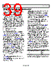
40 / 73 page  Data Sheet AD9142A SYNCHRONIZATION IMPLEMENTATION The AD9142A lets the user choose either the rising or falling edge of the DAC clock to sample the sync clock, which makes it easier to meet the timing requirements. Ensure that the sync clock, fSYNC, is 1/8 × fDATA or slower by a factor of 2n, n being an integer (1, 2, 3…). Note that there is a limit on how slow the sync clock can be received because of the ac coupling nature of the sync clock receiver. Choose an appropriate value of the ac coupling capacitors to ensure that the signal swing meets the data sheet specification, as listed in Table 2. The frame clock resets the FIFO in multiple AD9142A devices. The frame can be either a one shot or continuous clock. In either case, the pulse width of the frame must be longer than one DCI cycle in the word interface mode and two DCI cycles in the byte interface mode. When the frame is a continuous clock, fFRAME, ensure that it is 1/8 × fDATA or slower by a factor of 2n, n being an integer (1, 2, 3…). Table 23 lists the requirements of the frame clock in various conditions. Byte interface mode is not supported when the frame signal is used in synchronization. Table 23. Frame Clock Speed and Pulse Width Requirement Sync Clock Maximum Speed Minimum Pulse Width One Shot N/A1 For both one shot and continuous sync clocks, word interface mode = one DCI cycle and byte interface mode = two DCI cycles. Continuous fDATA/8 1 N/A means not applicable. SYNCHRONIZATION PROCEDURES When the sync accuracy of an application is less precise than two DAC clock cycles, it is recommended to turn off the synchro- nization machine because there are no additional steps required, other than the regular start-up procedure sequence. For applications that require more precise sync accuracy than two DAC clock cycles, it is recommended that the procedure in the Synchronization Procedure for PLL Off or Synchronization Procedure for PLL On sections be followed to set up the system and configure the device. For more information about the details of the synchronization scheme in the AD9142A and using the synchronization function to correct system skews and drifts, see the DAC Latency and System Skews section. Synchronization Procedure for PLL Off 1. Configure the DAC interpolation mode and, if NCO is used, configure the NCO FTW. 2. Set up the DAC data interface according to the procedure outlined in the Data Interface section and verify that the DLL is locked. 3. Choose the appropriate mode in the FRAME_RESET_MODE bits (Register 0x22[1:0]). a. If NCO is not used, choose FIFO only mode. b. If NCO is used, it must be synchronized. FIFO and NCO mode can then be used. 4. Configure Bit 2 in Register 0x22 for continuous or one shot reset mode. One shot reset mode is recommended. 5. Ensure that the DACCLK, DCI, and sync clock to all of the AD9142A devices are running and stable. 6. Enable the sync engine by writing 1 to Register 0x21[0]. 7. Send a valid frame pulse(s) to all of the AD9142A devices. 8. Verify that the frame pulse is received by each device by reading back Register 0x22[3]. All the readback values are 1. At this point, the devices should be synchronized. Synchronization Procedure for PLL On Note that, because the sync clock and PLL reference clock share the same clock and the maximum sync clock rate is fDATA/8, the same limit also applies to the reference clock. Therefore, only 2× interpolation is supported for synchronization with PLL on. 1. Set up the PLL according to the procedure in the Clock Multiplication section and ensure that the PLL is locked. 2. Configure the DAC interpolation mode and, if NCO is used, configure the NCO FTW. 3. Set up the DAC data interface according to the procedure in the Data Interface section and verify that the DLL is locked. 4. Choose the appropriate mode in the FRAME_RESET_MODE bits (Register 0x22[1:0]) a. If NCO is not used, choose the FIFO only mode. b. If NCO is used, it must be synchronized. FIFO and NCO mode can then be used. 5. Configure Bit 2 in Register 0x22 for continuous or one shot reset mode. One shot reset mode is recommended. 6. Ensure that DACCLK, DCI, and sync clock to all of the AD9142A devices are running. 7. Enable the sync engine by writing 1 to Register 0x21[0]. 8. Send a valid frame pulse(s) to all of the AD9142A devices. 9. Verify that the frame pulse is received by each device by reading back Register 0x22[3]. All the readback values are 1. At this point, the devices should be synchronized. Rev. A | Page 39 of 72 |
|
链接网址 |
| ALLDATASHEET是否为您带来帮助? [ DONATE ] |
关于 Alldatasheet | 广告服务 | 联系我们 | 隐私政策 | 数据表链接 | 链接交换 | 制造商名单 All Rights Reserved©Alldatasheet.com |
| Russian : Alldatasheetru.com | Korean : Alldatasheet.co.kr | Spanish : Alldatasheet.es | French : Alldatasheet.fr | Italian : Alldatasheetit.com Portuguese : Alldatasheetpt.com | Polish : Alldatasheet.pl | Vietnamese : Alldatasheet.vn Indian : Alldatasheet.in | Mexican : Alldatasheet.com.mx | British : Alldatasheet.co.uk | New Zealand : Alldatasheet.co.nz |
|
Family Site : ic2ic.com |
icmetro.com |
 Chinese ▼
 English
 Chinese
 German
 Japanese
 Russian
 Korean
 Spanish
 French
 Italian
 Portuguese
 Polish
 Vietnamese
 Indian
 Mexican
 British
 New Zealand