|
数据搜索系统,热门电子元器件搜索 |
|
|
数据搜索系统,热门电子元器件搜索 |
|
AD9142ABCPZ 数据表(PDF) 10 Page - Analog Devices |
|
|
|||||||||||||||||||||||||||||
AD9142ABCPZ 数据表(HTML) 10 Page - Analog Devices |
|
|
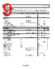
10 / 73 page  Data Sheet AD9142A DAC LATENCY SPECIFICATIONS TMIN to TMAX, AVDD33 = 3.3 V, DVDD18 = 1.8 V, CVDD18 = 1.8 V, IOUTFS = 20 mA, FIFO level is set to 4 (half of the FIFO depth), unless otherwise noted. Table 3. Parameter Test Conditions/Comments Min Typ Max Unit WORD INTERFACE MODE Fine/coarse modulation, inverse sinc, gain/phase compensation off 2× Interpolation 134 DACCLK cycles 4× Interpolation 244 DACCLK cycles 8× Interpolation 481 DACCLK cycles BYTE INTERFACE MODE Fine/coarse modulation, inverse sinc, gain/phase compensation off 2× Interpolation 145 DACCLK cycles 4× Interpolation 271 DACCLK cycles 8× Interpolation 506 DACCLK cycles INDIVIDUAL FUNCTION BLOCKS Modulation Fine 17 DACCLK cycles Coarse 10 DACCLK cycles Inverse Sinc 20 DACCLK cycles Phase Compensation 12 DACCLK cycles Gain Compensation 16 DACCLK cycles LATENCY VARIATION SPECIFICATIONS Table 4. Parameter Min Typ Max Unit DAC LATENCY VARIATION1 SYNC Off 1 2 DACCLK cycles SYNC On 0 1 DACCLK cycles 1 DAC latency is defined as the elapsed time from a data sample clocked at the input to the AD9142A until the analog output begins to change. Rev. A | Page 9 of 72 |
|
链接网址 |
| ALLDATASHEET是否为您带来帮助? [ DONATE ] |
关于 Alldatasheet | 广告服务 | 联系我们 | 隐私政策 | 数据表链接 | 链接交换 | 制造商名单 All Rights Reserved©Alldatasheet.com |
| Russian : Alldatasheetru.com | Korean : Alldatasheet.co.kr | Spanish : Alldatasheet.es | French : Alldatasheet.fr | Italian : Alldatasheetit.com Portuguese : Alldatasheetpt.com | Polish : Alldatasheet.pl | Vietnamese : Alldatasheet.vn Indian : Alldatasheet.in | Mexican : Alldatasheet.com.mx | British : Alldatasheet.co.uk | New Zealand : Alldatasheet.co.nz |
|
Family Site : ic2ic.com |
icmetro.com |
 Chinese ▼
 English
 Chinese
 German
 Japanese
 Russian
 Korean
 Spanish
 French
 Italian
 Portuguese
 Polish
 Vietnamese
 Indian
 Mexican
 British
 New Zealand