|
数据搜索系统,热门电子元器件搜索 |
|
|
数据搜索系统,热门电子元器件搜索 |
|
P9222-R 数据表(PDF) 32 Page - Renesas Technology Corp |
|
|
|||||||||||||||||||||||||||||
P9222-R 数据表(HTML) 32 Page - Renesas Technology Corp |
|
|
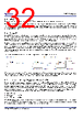
32 / 58 page  P9222-R/RN Datasheet © 2019-2022 Renesas Electronics Corporation 32 May 5, 2022 8.3 VRECT Pin The efficiency of the full-bridge rectifier in the P9222-R/RN is increased by implementing it as a synchronous rectifier. The rectifier comprises four self-driven switches that work in a full synchronous mode of operation when the load is higher than 150mA. Below that threshold, the rectifier works in half-synchronous rectification mode. At power-up, when the voltage is below the UVLO threshold, the rectifier works by using the body diodes associated with the NMOS transistors. The BST capacitors are used to provide power to drive the gates of high-side NMOS switches. 8.4 Enable Pin The P9222-R/RN offers an active LOW enable function that allows the host AP to control when wireless power will be enabled. The /EN enable pin (C4) must be actively pulled-up or pulled-down using the AP to drive the pin directly, or by using an external resistor to passively control the default state. The /EN pin is a push-pull general purpose input/output (GPIO) type input and will consume current when driven HIGH while the P9222-R/RN is not powered. It is recommended that one of the circuits shown in Figure 27 be followed. The /EN pin can be actively controlled (AP I/O directly connected to /EN pin) or passively controlled depending on system requirements. Since the AP must be used to control the P9222-R/RN enable pin, power will be consumed by the biasing resistor when the state is changed from the default if using a passive control scheme – this may be needed to support AP sleep modes. Typical systems will use the P9222-R/RN set up to be enabled by default in order to save the most power, and will disable wireless charging when wired charging is used or some other function is being performed that requires wireless charging to remain disabled. One of the diagrams in Figure 27 must be used to set the default /EN pin state for the P9222-R/RN. Figure 27. P9222-R/RN Recommended Enable Default State Configurations When using the “active enable control,” it is important to always force the /EN pin into a known state, and the /EN pin should never be left floating. For example, in some applications when the battery is dead or when the AP is in sleep mode, the AP may not be actively driving the /EN pin. In order to prevent the /EN pin from floating in such cases, a pull-down resistor should be added. 8.5 Transient Voltage Suppressor Diodes (TVS) Transient Voltage Suppressor diodes can be added to the design from the AC1 and AC2 nodes to GND, or from AC1 to AC2 (D10, D2, D3, as shown in the reference schematic). This component is useful to rapidly limit incoming ESD surges, or situations when the Tx incoming power exceeds the expected power and Vrect voltage rises above target and over 15V in less than 10µs to aid in voltage limiting the incoming AC waveforms. A balance in Reverse Standoff Voltage (VRWM), Clamping Voltage (VCL), Break-down Voltage (VBR) relative to the expected Vrect operating voltage Vrect (be sure minimum VBR is less than maximum operating Vrect value and that VCL is less than Vrect Absolute maximum voltage) should be reached. The following guidance should be used for the P9222-R/RN when selecting TVS diodes: VRWM = 12V maximum VBR = 14.6 V minimum at 5mA VCL = 22 V maximum at 1App When TVS diodes are used, it is recommended to place them as close to the coil on the respective nodes as possible to shunt high voltages away from the P9222-R/RN. Zener diodes can also be used to limit voltage levels, and the Zener voltage should be above the working voltage of the node and below the absolute maximum voltage of the pin connected to the node. |
|
链接网址 |
| ALLDATASHEET是否为您带来帮助? [ DONATE ] |
关于 Alldatasheet | 广告服务 | 联系我们 | 隐私政策 | 数据表链接 | 链接交换 | 制造商名单 All Rights Reserved©Alldatasheet.com |
| Russian : Alldatasheetru.com | Korean : Alldatasheet.co.kr | Spanish : Alldatasheet.es | French : Alldatasheet.fr | Italian : Alldatasheetit.com Portuguese : Alldatasheetpt.com | Polish : Alldatasheet.pl | Vietnamese : Alldatasheet.vn Indian : Alldatasheet.in | Mexican : Alldatasheet.com.mx | British : Alldatasheet.co.uk | New Zealand : Alldatasheet.co.nz |
|
Family Site : ic2ic.com |
icmetro.com |
 Chinese ▼
 English
 Chinese
 German
 Japanese
 Russian
 Korean
 Spanish
 French
 Italian
 Portuguese
 Polish
 Vietnamese
 Indian
 Mexican
 British
 New Zealand