|
数据搜索系统,热门电子元器件搜索 |
|
|
数据搜索系统,热门电子元器件搜索 |
|
P9222-R 数据表(PDF) 9 Page - Renesas Technology Corp |
|
|
|||||||||||||||||||||||||||||
P9222-R 数据表(HTML) 9 Page - Renesas Technology Corp |
|
|
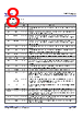
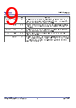
9 / 58 page  P9222-R/RN Datasheet © 2019-2022 Renesas Electronics Corporation 9 May 5, 2022 Pin Number Name Type Description F2, G1, G2 AC1 Input AC power input 1. Connect AC1 to the CS capacitors and CS to the Rx coil. Connect the CD capacitor from AC1 to AC2 (see Figure 2 and the application schematic in Figure 36). Due to symmetry, the AC1 and AC2 connections are interchangeable. F3 PDETB Output Open-drain, active-LOW. This pin is an output for indicating ping events are being received by the Rx. Connect this pin to the application processor (AP) I/O voltage rail using an external pull-up resistor. F4, G4, G5 AC2 Input AC power input 2. Connect this pin to the Rx coil and the CD capacitor (see Figure 2) Due to symmetry, the AC1 and AC2 connections are interchangeable.) F5 BST2 Output Bootstrap capacitor for driving the high-side NFETs of the internal rectifier. Connect a 15nF capacitor from AC2 to BST2. G3 PDET_RC Input Ping-detect input pin for determining when PDETB will be de-asserted. This pin is used to notify the AP if the Rx device is removed from the power transfer interface. Connect an RC time-delay circuit designed to hold the voltage on this pin above VPDET_RC_IL between each Tx ping after power transfer is completed (EOC). |
|
链接网址 |
| ALLDATASHEET是否为您带来帮助? [ DONATE ] |
关于 Alldatasheet | 广告服务 | 联系我们 | 隐私政策 | 数据表链接 | 链接交换 | 制造商名单 All Rights Reserved©Alldatasheet.com |
| Russian : Alldatasheetru.com | Korean : Alldatasheet.co.kr | Spanish : Alldatasheet.es | French : Alldatasheet.fr | Italian : Alldatasheetit.com Portuguese : Alldatasheetpt.com | Polish : Alldatasheet.pl | Vietnamese : Alldatasheet.vn Indian : Alldatasheet.in | Mexican : Alldatasheet.com.mx | British : Alldatasheet.co.uk | New Zealand : Alldatasheet.co.nz |
|
Family Site : ic2ic.com |
icmetro.com |
 Chinese ▼
 English
 Chinese
 German
 Japanese
 Russian
 Korean
 Spanish
 French
 Italian
 Portuguese
 Polish
 Vietnamese
 Indian
 Mexican
 British
 New Zealand