|
数据搜索系统,热门电子元器件搜索 |
|
|
数据搜索系统,热门电子元器件搜索 |
|
P9222-R 数据表(PDF) 8 Page - Renesas Technology Corp |
|
|
|||||||||||||||||||||||||||||
P9222-R 数据表(HTML) 8 Page - Renesas Technology Corp |
|
|
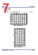
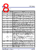
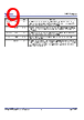
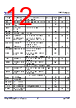
8 / 58 page  P9222-R/RN Datasheet © 2019-2022 Renesas Electronics Corporation 8 May 5, 2022 1.2 Pin Descriptions Table 1. Pin Descriptions Pin Number Name Type Description A1 CM1 Output High-voltage, open-drain output from the modulation FETs. Connect a 47nF capacitor from AC1 to CM1. A2 OD2 Input/Output Open-drain GPIO. This pin is connected to the internal ADC and can measure voltages smaller than 1.2V. This pin can be left floating if not used. A3 OD0/SCL Input/Output Open-drain GPIO. This pin supports an input of up to 5V, and is used for the I2C SCL connection. Connect this pin via a pull-up resistor to the system I/O supply. This pin can be left floating if not used. A4 OD1/SDA Input/Output Open-drain GPIO. This pin supports an input of up to 5V, and is used for the I2C SDA connection. Connect this pin via a pull-up resistor to the system I/O supply. This pin can be left floating if not used. A5 CM2 Output High-voltage, open-drain output from the modulation FETs. Connect a 47nF capacitor from AC2 to CM2. B1 CMA Output High-voltage, open-drain output from the modulation FETs. By default, CMA capacitor is not used for communication. This pin can be left floating if not used. B2 GP1/ADC IN Input/Output GPIO1. Pin is connected to internal ADC and can measure system voltage smaller than 1.8V. During startup this pin is set as a high-impedance. This pin can be left floating if not used. B3, H1-H5 PGND GND Power and logic ground. B4 /INT Output Interrupt output pin. Connect this pin to the application processor (AP) I/O voltage rail using an external pull-up resistor. The P9222-R/RN drives this pin LOW to notify the AP host of status changes. B5 CMB Output High-voltage, open-drain modulation FETs. By default, CMB capacitor is not used for communication. This pin can be left floating if not used. C1 LDO5P0 Output Internal 5V LDO for chip power only. Connect a 1µF and 0.1µF capacitor to ground. C2 GP2 Input GPIO2. If this pin is pulled high to the internal 1.8V LDO (LDO1P8) using a 10K resistor, the P9222-R/RN becomes an I2C master during startup to load 100 bytes of user configuration from external EEPROM. If this pin is pulled to ground, the P9222-R/RN loads the default configuration from the internal OTP. C3 GP0/ Thermistor Input/Output GPIO0. This pin can be used to measure coil temperature. The P9222-R/RN interrupts the processor when the coil voltage goes below 0.6V. During the startup this pin is set as a high- impedance. Pull this pin to 1.8V with a resistor if not used. C4 /EN Input Active-LOW enable pin. To enable the P9222-R/RN, pull this pin to GND. To disable the P9222- R/RN, pull this pin High. C5 LDO1P8 Output Internal 1.8V LDO output for logic power. Connect a 1µF and 0.1µF capacitor to ground. D1-D5 VOUT Output Main LDO output pin. Connect at least a 1×10µF capacitor from this pin to ground. It is not recommended to directly connect the USB charging port or other voltage sources to these pins. Back-to-back isolation FETs are recommended. E1-E5 VRECT Input/Output Filter capacitor for the internal rectifier. Capacitance requirements: Connect 2×10µF and 1×0.1µF capacitors in parallel from this pin to ground. F1 BST1 Output Bootstrap capacitor for driving the high side NFETs of the internal rectifier. Connect a 15nF capacitor from AC1 to BST1. |
|
链接网址 |
| ALLDATASHEET是否为您带来帮助? [ DONATE ] |
关于 Alldatasheet | 广告服务 | 联系我们 | 隐私政策 | 数据表链接 | 链接交换 | 制造商名单 All Rights Reserved©Alldatasheet.com |
| Russian : Alldatasheetru.com | Korean : Alldatasheet.co.kr | Spanish : Alldatasheet.es | French : Alldatasheet.fr | Italian : Alldatasheetit.com Portuguese : Alldatasheetpt.com | Polish : Alldatasheet.pl | Vietnamese : Alldatasheet.vn Indian : Alldatasheet.in | Mexican : Alldatasheet.com.mx | British : Alldatasheet.co.uk | New Zealand : Alldatasheet.co.nz |
|
Family Site : ic2ic.com |
icmetro.com |
 Chinese ▼
 English
 Chinese
 German
 Japanese
 Russian
 Korean
 Spanish
 French
 Italian
 Portuguese
 Polish
 Vietnamese
 Indian
 Mexican
 British
 New Zealand