|
数据搜索系统,热门电子元器件搜索 |
|
|
数据搜索系统,热门电子元器件搜索 |
|
P9222-R 数据表(PDF) 4 Page - Renesas Technology Corp |
|
|
|||||||||||||||||||||||||||||
P9222-R 数据表(HTML) 4 Page - Renesas Technology Corp |
|
|
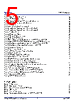
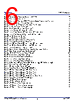
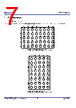
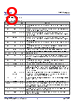
4 / 58 page  P9222-R/RN Datasheet © 2019-2022 Renesas Electronics Corporation 4 May 5, 2022 8. Applications Information .............................................................................................................................................................................31 8.1 Receiver Coil....................................................................................................................................................................................31 8.2 Series and Parallel Resonant Capacitor Selection...........................................................................................................................31 8.3 VRECT Pin.......................................................................................................................................................................................32 8.4 Enable Pin........................................................................................................................................................................................32 8.5 Transient Voltage Suppressor Diodes (TVS)...................................................................................................................................32 8.6 GPIO Pins........................................................................................................................................................................................33 8.6.1 OD0 Pin..............................................................................................................................................................................33 8.6.2 OD1 Pin..............................................................................................................................................................................33 8.6.3 OD2 Pin..............................................................................................................................................................................33 8.6.4 GP0 Pin ..............................................................................................................................................................................33 8.6.5 GP1 Pin ..............................................................................................................................................................................33 8.6.6 GP2 Pin ..............................................................................................................................................................................34 8.7 Low-Power Ping Detection Operation..............................................................................................................................................34 8.8 Configuration of P9222-R/RN Parameters.......................................................................................................................................36 8.9 P9222-R/RN Internal Register Access by Application Processor ....................................................................................................36 8.10 External EEPROM Access by P9222-R/RN.....................................................................................................................................36 9. Examples of User Customizing P9222-R/RN Operating Parameters.........................................................................................................37 9.1 LDO Output Voltage (VOUT) Configuration.....................................................................................................................................37 9.1.1 VOUT Adjustment via the I2C Interface .............................................................................................................................37 9.1.2 VOUT Configuration Change Using an External EEPROM................................................................................................38 9.2 Current Limit (ILIM) Configuration....................................................................................................................................................38 9.3 Overvoltage (OV) Protection Configuration......................................................................................................................................39 9.4 FOD (Foreign Object Detection) ......................................................................................................................................................39 9.4.1 Configuring FOD Parameters.............................................................................................................................................40 9.4.2 Modulation Capacitor and Interrupt Enables ......................................................................................................................41 10. I2C Function ...............................................................................................................................................................................................42 11. Registers ....................................................................................................................................................................................................42 12. Application Schematic ................................................................................................................................................................................53 13. Package Outline Drawings .........................................................................................................................................................................54 14. Marking Diagram ........................................................................................................................................................................................54 15. Ordering Information...................................................................................................................................................................................54 16. Revision History..........................................................................................................................................................................................55 List of Figures Figure 1. Simplified Block Diagram.....................................................................................................................................................................1 Figure 2. P9222-R/RN Block and Application Diagram ......................................................................................................................................2 Figure 3. Pin Assignments for 40-WLCSP (AZG40), 2.28 × 3.38 mm with 0.4mm Pitch – Top View.................................................................7 Figure 4. Block Diagram of WPC Compliant Wireless Power Transfer System ...............................................................................................15 |
|
链接网址 |
| ALLDATASHEET是否为您带来帮助? [ DONATE ] |
关于 Alldatasheet | 广告服务 | 联系我们 | 隐私政策 | 数据表链接 | 链接交换 | 制造商名单 All Rights Reserved©Alldatasheet.com |
| Russian : Alldatasheetru.com | Korean : Alldatasheet.co.kr | Spanish : Alldatasheet.es | French : Alldatasheet.fr | Italian : Alldatasheetit.com Portuguese : Alldatasheetpt.com | Polish : Alldatasheet.pl | Vietnamese : Alldatasheet.vn Indian : Alldatasheet.in | Mexican : Alldatasheet.com.mx | British : Alldatasheet.co.uk | New Zealand : Alldatasheet.co.nz |
|
Family Site : ic2ic.com |
icmetro.com |
 Chinese ▼
 English
 Chinese
 German
 Japanese
 Russian
 Korean
 Spanish
 French
 Italian
 Portuguese
 Polish
 Vietnamese
 Indian
 Mexican
 British
 New Zealand