|
数据搜索系统,热门电子元器件搜索 |
|
|
数据搜索系统,热门电子元器件搜索 |
|
P9222-R 数据表(PDF) 42 Page - Renesas Technology Corp |
|
|
|||||||||||||||||||||||||||||
P9222-R 数据表(HTML) 42 Page - Renesas Technology Corp |
|
|
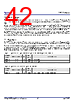
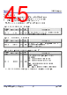
42 / 58 page  P9222-R/RN Datasheet © 2019-2022 Renesas Electronics Corporation 42 May 5, 2022 10. I2C Function The P9222-R/RN uses the standard I2C slave implementation protocol to communicate with a host AP or other I2C peripherals. The communication protocol is implemented by using 8 bits for data and 16 bits for addresses. The default slave address of the P9222-R/RN is 0x61h. When writing to the P9222-R/RN, care should be taken to only write to registers marked exclusively as Read/Write (RW). Registers marked as Read Only (R) should never be sent a Write command or unexpected behavior may occur. In addition, register locations marked Reserved should not receive a Write command. When writing to a RW register that contains a combination of RW fields and reserved fields, a read- modify-write should be performed to the intended bit/field only. All other bits/field, including reserved bits/fields, should NOT be modified. The P9222-R/RN Rx device operates in Rx mode. Depending on the firmware (FW) loaded into OTP memory or updated by the AP, the P9222- R/RN Rx will follow the programmed settings once connected wirelessly to a Tx. Some registers are defined and implemented for Read-only, some registers are Read/Write, and some registers are volatile and will be reset if power is cycled. 11. Registers The P9222-R/RN uses the standard I2C slave implementation protocol to communicate with a host AP or other I2C peripherals. The communication protocol is implemented using 8 bits for data and 16 bits for addresses. The default slave address of the P9222-R/RN is 0x61. The following tables list address locations, field names, available operations (R or RW), default values, and functional descriptions of internally accessible registers contained within the P9222-R/RN. The OTP registers are loaded each time the device is powered and cannot be changed except by new firmware programmed into a blank device. The SRAM registers are available to make setting changes after the device is powered. These changes are reset to default when the power is cycled or the device is reset. Table 11. Chip Part Number ID Register, Chip_ID_L (0x00), Chip_ID_H (0x01) Address and Bit Register Field Name R/W Default Value Function and Description 0x00 [7:0] Chip_ID_L R 0x22 Chip ID low byte 0x01 [7:0] Chip_ID_H R 0x92 Chip ID high byte Table 12. Chip Revision Register, Chip_Rev (0x02) Address and Bit Register Field Name R/W Default Value Function and Description 0x02 [7:0] Chip_Rev R 0x02 Chip main revision. Latest chip revision is 0x02 (default). |
|
链接网址 |
| ALLDATASHEET是否为您带来帮助? [ DONATE ] |
关于 Alldatasheet | 广告服务 | 联系我们 | 隐私政策 | 数据表链接 | 链接交换 | 制造商名单 All Rights Reserved©Alldatasheet.com |
| Russian : Alldatasheetru.com | Korean : Alldatasheet.co.kr | Spanish : Alldatasheet.es | French : Alldatasheet.fr | Italian : Alldatasheetit.com Portuguese : Alldatasheetpt.com | Polish : Alldatasheet.pl | Vietnamese : Alldatasheet.vn Indian : Alldatasheet.in | Mexican : Alldatasheet.com.mx | British : Alldatasheet.co.uk | New Zealand : Alldatasheet.co.nz |
|
Family Site : ic2ic.com |
icmetro.com |
 Chinese ▼
 English
 Chinese
 German
 Japanese
 Russian
 Korean
 Spanish
 French
 Italian
 Portuguese
 Polish
 Vietnamese
 Indian
 Mexican
 British
 New Zealand