|
数据搜索系统,热门电子元器件搜索 |
|
|
数据搜索系统,热门电子元器件搜索 |
|
STCMB1 数据表(PDF) 8 Page - STMicroelectronics |
|
|
|||||||||||||||||||||||||||||
STCMB1 数据表(HTML) 8 Page - STMicroelectronics |
|
|
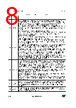
8 / 59 page  Pin connections and description STCMB1 8/59 DocID028958 Rev 4 10 STBY Burst mode operation threshold for the HB. The pin senses some voltage related to the feedback control, which is compared to an internal reference (1.25 V). If the voltage on the pin is lower than the reference, the IC stops switching, enters an idle state and its quiescent current is reduced. The chip restarts switching as the voltage exceeds the reference by 40 mV. Soft-start is not invoked. When the HB is stopped the PFC is stopped as well; while the HB is switching the PFC stage is enabled and it switches or not depending on the level of the COMP pin. Tie the pin to RFMIN if the burst mode operation is not used. An RC filter is mandatory, with R > 100 and C > 100 pF. Please note that the time constant of the RC filter enters in the loop transfer function, when the pin is directly fed by the phototransistor of the optocoupler. 11 ISEN_PFC The inductor current is sensed through a resistor RS on the current return side and the resulting negative voltage is applied to this pin through a limiting resistor. When the power MOSFET is turned on an internal comparator enables the PWM ramp to start only when the voltage on the pin is lower than -25 mV (typical value), e.g.: when the inductor current is slightly positive. If the voltage on the pin goes below -0.5 V the internal overcurrent comparator is triggered and terminates the conduction cycle of the external power MOSFET before the normal PWM circuit does. In this way, the peak inductor current is limited at a maximum of 0.5/RS. A voltage on this pin higher than -25 mV (typical value) enables both power MOSFET's turn-on when a cycle is initiated by the demagnetization sensing circuit and when it is initiated by the internal starter. In this way, the unit stops during the current surges occurring at power up or after a mains dip or a missing cycle and restarts switching only when the surge is over. An RC filter is mandatory at the pin, R > 100 and C > 100 pF. The overall time constant should give a negligible delay with respect to the typical operating frequencies of the PFC. The value of the resistor also defines the effect of the THD optimizer (enhanced COT): THD is usually optimized with a value between 100 and 300 12 ISEN_HB Current sense input for the HB. The pin senses the resonant current through a sense resistor or a capacitive divider for lossless sensing. If the voltage exceeds a 0.8 V threshold the soft-start capacitor connected to the CSS pin is internally discharged: the frequency increases hence limiting the power throughput. Under the output short-circuit, this normally results in a nearly constant peak primary current. This condition is allowed for a maximum time internally set at 40 ms minimum. If the current keeps on building up despite this frequency increase, a second comparator referenced to 1.5 V disables switching immediately. In both cases VCC is recycled before restarting (see the HV pin). As long as the voltage on the CSS pin is lower than 0.3 V, this second comparator is inhibited. The pin is used also by the hard switching prevention (HSP) function. Do not short the pin to ground; this would prevent the device from operating correctly. An RC filter is recommended to reduce the noise level at the pin, with R > 50 and C > 100 pF. The overall time constant should give a negligible delay with respect to the typical operating frequencies of the LLC. 13 GND Ground. Current return for signal parts of the IC, the PFC gate driver and the low-side gate driver of the half-bridge. Keep the PCB trace that goes from this pin to the sources of the PFC and the low-side MOSFETs separate from the trace that collects the grounding of the bias components. 14 GD_PFC PFC gate driver output. The totem pole output stage is able to drive power MOSFETs and IGBTs. It is capable of a 0.6 A source current and a 0.8 A sink current (minimum values). The pin is actively pulled to GND during UVLO. Table 1. Pin description (continued) Pin no. Name Function |
|
链接网址 |
| ALLDATASHEET是否为您带来帮助? [ DONATE ] |
关于 Alldatasheet | 广告服务 | 联系我们 | 隐私政策 | 数据表链接 | 链接交换 | 制造商名单 All Rights Reserved©Alldatasheet.com |
| Russian : Alldatasheetru.com | Korean : Alldatasheet.co.kr | Spanish : Alldatasheet.es | French : Alldatasheet.fr | Italian : Alldatasheetit.com Portuguese : Alldatasheetpt.com | Polish : Alldatasheet.pl | Vietnamese : Alldatasheet.vn Indian : Alldatasheet.in | Mexican : Alldatasheet.com.mx | British : Alldatasheet.co.uk | New Zealand : Alldatasheet.co.nz |
|
Family Site : ic2ic.com |
icmetro.com |
 Chinese ▼
 English
 Chinese
 German
 Japanese
 Russian
 Korean
 Spanish
 French
 Italian
 Portuguese
 Polish
 Vietnamese
 Indian
 Mexican
 British
 New Zealand