|
数据搜索系统,热门电子元器件搜索 |
|
|
数据搜索系统,热门电子元器件搜索 |
|
ADAR4002ACPZ-R7 数据表(PDF) 52 Page - Analog Devices |
|
|
|||||||||||||||||||||||||||||
ADAR4002ACPZ-R7 数据表(HTML) 52 Page - Analog Devices |
|
|
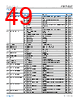
52 / 66 page  Data Sheet ADAR4002 REGISTER MAP analog.com Rev. A | 52 of 66 Table 14. ADAR4002 Register Summary (Continued) Addr Name Bits Bit Name Description Reset Access 0 DATA_LOAD Load Signal for Second Rank of Registers. This bit auto clears after being set. 0x0 R/W 0x36 TD11 7 FR_TDRANGE11 Time Delay Range. 0 = Range 0, 508 ps, and 1 = Range 1, 254 ps. 0x0 R/W [6:0] FIRSTRANK_TIMEDELAY11 7-Bit Time Delay Control. Default = 0x00, minimum time delay. 0x0 R/W 0x37 DSA11 [7:2] FIRSTRANK_DSA11 6-Bit Attenuation Control. Default = 0x3F, maximum attenuation. 0x3F R/W 1 RESERVED Reserved. 0x0 R 0 DATA_LOAD Load Signal for Second Rank of Registers. This bit auto clears after being set. 0x0 R/W 0x38 TD12 7 FR_TDRANGE12 Time Delay Range. 0 = Range 0, 508 ps, and 1 = Range 1, 254 ps. 0x0 R/W [6:0] FIRSTRANK_TIMEDELAY12 7-Bit Time Delay Control. Default = 0x00, minimum time delay. 0x0 R/W 0x39 DSA12 [7:2] FIRSTRANK_DSA12 6-Bit Attenuation Control. Default = 0x3F, maximum attenuation. 0x3F R/W 1 RESERVED Reserved. 0x0 R 0 DATA_LOAD Load Signal for Second Rank of Registers. This bit auto clears after being set. 0x0 R/W 0x3A TD13 7 FR_TDRANGE13 Time Delay Range. 0 = Range 0, 508 ps, and 1 = Range 1, 254 ps. 0x0 R/W [6:0] FIRSTRANK_TIMEDELAY13 7-Bit Time Delay Control. Default = 0x00, minimum time delay. 0x0 R/W 0x3B DSA13 [7:2] FIRSTRANK_DSA13 6-Bit Attenuation Control. Default = 0x3F, maximum attenuation. 0x3F R/W 1 RESERVED Reserved. 0x0 R 0 DATA_LOAD Load Signal for Second Rank of Registers. This bit auto clears after being set. 0x0 R/W 0x3C TD14 7 FR_TDRANGE14 Time Delay Range. 0 = Range 0, 508 ps, and 1 = Range 1, 254 ps. 0x0 R/W [6:0] FIRSTRANK_TIMEDELAY14 7-Bit Time Delay Control. Default = 0x00, minimum time delay. 0x0 R/W 0x3D DSA14 [7:2] FIRSTRANK_DSA14 6-Bit Attenuation Control. Default = 0x3F, maximum attenuation. 0x3F R/W 1 RESERVED Reserved. 0x0 R 0 DATA_LOAD Load Signal for Second Rank of Registers. This bit auto clears after being set. 0x0 R/W 0x3E TD15 7 FR_TDRANGE15 Time Delay Range. 0 = Range 0, 508 ps, and 1 = Range 1, 254 ps. 0x0 R/W [6:0] FIRSTRANK_TIMEDELAY15 7-Bit Time Delay Control. Default = 0x00, minimum time delay. 0x0 R/W 0x3F DSA15 [7:2] FIRSTRANK_DSA15 6-Bit Attenuation Control. Default = 0x3F, maximum attenuation. 0x3F R/W 1 RESERVED Reserved. 0x0 R 0 DATA_LOAD Load Signal for Second Rank of Registers. This bit auto clears after being set. 0x0 R/W 0x40 TD16 7 FR_TDRANGE16 Time Delay Range. 0 = Range 0, 508 ps, and 1 = Range 1, 254 ps. 0x0 R/W [6:0] FIRSTRANK_TIMEDELAY16 7-Bit Time Delay Control. Default = 0x00, minimum time delay. 0x0 R/W |
|
链接网址 |
| ALLDATASHEET是否为您带来帮助? [ DONATE ] |
关于 Alldatasheet | 广告服务 | 联系我们 | 隐私政策 | 数据表链接 | 链接交换 | 制造商名单 All Rights Reserved©Alldatasheet.com |
| Russian : Alldatasheetru.com | Korean : Alldatasheet.co.kr | Spanish : Alldatasheet.es | French : Alldatasheet.fr | Italian : Alldatasheetit.com Portuguese : Alldatasheetpt.com | Polish : Alldatasheet.pl | Vietnamese : Alldatasheet.vn Indian : Alldatasheet.in | Mexican : Alldatasheet.com.mx | British : Alldatasheet.co.uk | New Zealand : Alldatasheet.co.nz |
|
Family Site : ic2ic.com |
icmetro.com |
 Chinese ▼
 English
 Chinese
 German
 Japanese
 Russian
 Korean
 Spanish
 French
 Italian
 Portuguese
 Polish
 Vietnamese
 Indian
 Mexican
 British
 New Zealand