|
数据搜索系统,热门电子元器件搜索 |
|
|
数据搜索系统,热门电子元器件搜索 |
|
RC19302A00AGNT#KD0 数据表(PDF) 44 Page - Renesas Technology Corp |
|
|
|||||||||||||||||||||||||||||
RC19302A00AGNT#KD0 数据表(HTML) 44 Page - Renesas Technology Corp |
|
|
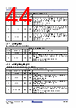
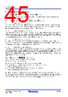
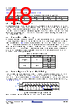
44 / 62 page  R31DS0210EU0106 Rev.1.06 Page 44 May 11, 2026 RC193xx Datasheet 4.5.17 WRITE_LOCK Non-clearable SMBus Write Lock Register. 4.5.18 WRITE_LOCK_LOS_EVT Clearable SMBus Write Lock and LOS Event Register. 2 rx_term1 RW 0x0 Enable internal termination for CLKIN1. Applications requiring receiver terminations may set this bit to enable internal termination resistors to ground on both the CLKIN1 and CLKIN1b pins. PCIe applications generally require Rx_TERM to be 0. 0 = Disable internal termination (PCIe) 1 = Enable internal termination 1 ac_in0 RW 0x0 AC-couple CLKIN0. When AC-coupling the input clock, set this bit to enable internal bias circuitry on the CLKIN0. This eliminates the need for external bias components on the CLKIN0 side of the AC-coupling capacitor. 0 = Disable internal bias (DC-coupled) 1 = Enable internal bias (AC-coupled) 0 rx_term0 RW 0x0 Enable internal termination for CLKIN0. Applications requiring receiver terminations may set this bit to enable internal termination resistors to ground on both the CLKIN0 and CLKIN0b pins. PCIe applications generally require Rx_TERM to be 0. 0 = Disable internal termination (PCIe) 1 = Enable internal termination WRITE_LOCK Bit Field Descriptions Bit Field Field Name Field Type Default Value Description 7:1 reserved RW 0x0 Reserved 0 write_lock RW 0x0 Non-clearable SMBus write lock bit. When written to one, the SMBus control registers cannot be written. They may be read. This bit can only be cleared by cycling power. 0 = SMBus writes are not prohibited by WRITE_LOCK 1 = SMBus locked for writing WRITE_LOCK_LOS_EVT Bit Field Descriptions Bit Field Field Name Field Type Default Value Description 7:3 reserved RW1C 0x0 Reserved 2 los1_evt RW1C 0x0 CLKIN1 LOS event sticky bit. When high, indicates that an LOS event was detected on CLKIN1. Can be cleared by writing a 1 to it. 0 = No LOS1 event detected 1 = LOS1 event detected. 1 los0_evt RW1C 0x0 CLKIN0 LOS event sticky bit. When high, indicates that an LOS event was detected on CLKIN0. Can be cleared by writing a 1 to it. 0 = No LOS event detected 1 = LOS event detected. 0 write_lock_rw1c RW1C 0x0 Clearable SMBus write lock bit. When written to one, the SMBus control registers cannot be written. They may be read. This bit can only be cleared by writing a 1 to it. 0 = SMBus writes are not prohibited by WRITE_LOCK_RW1C 1 = SMBus locked for writing RECEIVER_CONTROL Bit Field Descriptions Bit Field Field Name Field Type Default Value Description |
|
链接网址 |
| ALLDATASHEET是否为您带来帮助? [ DONATE ] |
关于 Alldatasheet | 广告服务 | 联系我们 | 隐私政策 | 数据表链接 | 链接交换 | 制造商名单 All Rights Reserved©Alldatasheet.com |
| Russian : Alldatasheetru.com | Korean : Alldatasheet.co.kr | Spanish : Alldatasheet.es | French : Alldatasheet.fr | Italian : Alldatasheetit.com Portuguese : Alldatasheetpt.com | Polish : Alldatasheet.pl | Vietnamese : Alldatasheet.vn Indian : Alldatasheet.in | Mexican : Alldatasheet.com.mx | British : Alldatasheet.co.uk | New Zealand : Alldatasheet.co.nz |
|
Family Site : ic2ic.com |
icmetro.com |
 Chinese ▼
 English
 Chinese
 German
 Japanese
 Russian
 Korean
 Spanish
 French
 Italian
 Portuguese
 Polish
 Vietnamese
 Indian
 Mexican
 British
 New Zealand