|
数据搜索系统,热门电子元器件搜索 |
|
|
数据搜索系统,热门电子元器件搜索 |
|
RC19302A00AGNT#KD0 数据表(PDF) 25 Page - Renesas Technology Corp |
|
|
|||||||||||||||||||||||||||||
RC19302A00AGNT#KD0 数据表(HTML) 25 Page - Renesas Technology Corp |
|
|
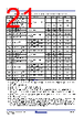
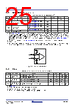
25 / 62 page  R31DS0210EU0106 Rev.1.06 Page 25 May 11, 2026 RC193xx Datasheet 2.4.5 CLKIN AC/DC Characteristics Figure 8. Clock Input Bias Network 2.4.6 Skew Table 22. CLKIN AC/DC Characteristics for DC-Coupled Operation[1] 1. See the Additive Phase Jitter tables for values required for performance. The CLKIN is designed for a ground-referenced differential input where the cross over voltage is approximately half of the swing. For example, a differential clock with a VOH of 1.2V would ideally have a crossover voltage of approximately 600mV. For applications where the input clock is not ground-referenced (LVPECL for example), the input clock needs to be AC-coupled and re-biased. Each RC193xx CLKIN has an internal bias circuit that may be enabled as well as internal terminations that may also be enabled. This reduces external components for such scenarios to a single external AC-coupling capacitor. See the RECEIVER_CONTROL register for details. Symbol Parameter Condition Minimum Typical Maximum Unit VIHMAX Maximum Input Voltage Single-ended value. - - 1.2 V VCROSS Input Crossover Voltage LOW_LOW_DETECT enabled (default value). [2] 2. Low/Low is an invalid differential state. LOW_LOW_DETECT allows the receiver turn itself off when such a condition is detected 131 - - mV LOW_LOW_DETECT disabled. 100 - - mV VSWING Input Swing [3] 3. Differential value. LOW_LOW_DETECT enabled (default value). [2] 528 - - mV LOW_LOW_DETECT disabled. 200 - - mV dv/dt Input Slew Rate [3][4] 4. Measured from -150mV to +150mV on the differential waveform (derived from REFCLK+ minus REFCLK-). The signal must be monotonic through the measurement region for rise and fall time. The 300mV measurement window is centered on the differential zero-crossing. - 0.6 - - V/ns Table 23. Output-to-Output and Input-to-Output Skew [1] 1. See Test Loads. Symbol Parameter Conditions Minimum Typical Maximum Unit tSK Output-to-Output Skew [2] 2. This parameter is defined in accordance with JEDEC Standard 65. Any two outputs in the same Bank. - 14 50 ps Any two outputs regardless of Bank.[3] 3. Output banks sourced from the same input. CLKSEL_tri = 0 or 1. - 25 60 ps tPD Input-to-Output Delay [4] 4. Defined as the time between to output rising edge and the input rising edge that caused it. Clock in to any output. Double-terminated. 0.9 1.1 1.3 ns Clock in to any output. Source-terminated. 0.9 1.1 1.7 ns tPD Input-to-Output Delay Variation [3] A single device, over temperature and voltage. - 1.3 2 ps/°C CLKIN CLKINb ~500mV |
|
链接网址 |
| ALLDATASHEET是否为您带来帮助? [ DONATE ] |
关于 Alldatasheet | 广告服务 | 联系我们 | 隐私政策 | 数据表链接 | 链接交换 | 制造商名单 All Rights Reserved©Alldatasheet.com |
| Russian : Alldatasheetru.com | Korean : Alldatasheet.co.kr | Spanish : Alldatasheet.es | French : Alldatasheet.fr | Italian : Alldatasheetit.com Portuguese : Alldatasheetpt.com | Polish : Alldatasheet.pl | Vietnamese : Alldatasheet.vn Indian : Alldatasheet.in | Mexican : Alldatasheet.com.mx | British : Alldatasheet.co.uk | New Zealand : Alldatasheet.co.nz |
|
Family Site : ic2ic.com |
icmetro.com |
 Chinese ▼
 English
 Chinese
 German
 Japanese
 Russian
 Korean
 Spanish
 French
 Italian
 Portuguese
 Polish
 Vietnamese
 Indian
 Mexican
 British
 New Zealand