|
数据搜索系统,热门电子元器件搜索 |
|
|
数据搜索系统,热门电子元器件搜索 |
|
RC19302A00AGNT#KD0 数据表(PDF) 49 Page - Renesas Technology Corp |
|
|
|||||||||||||||||||||||||||||
RC19302A00AGNT#KD0 数据表(HTML) 49 Page - Renesas Technology Corp |
|
|
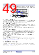
49 / 62 page  R31DS0210EU0106 Rev.1.06 Page 49 May 11, 2026 RC193xx Datasheet The following diagram shows the LOSb assertion sequence when the selected CLKIN is lost. It also shows the Automatic Clock Parking (ACP) circuit bring the outputs to a Low/Low state after an LOS event. For exact timing, see Electrical Characteristics. Figure 23. LOSb Assert Timing 5.7 Output Enable Control The RC193xx buffer/mux family provides two mechanisms to enable or disable clock outputs. Both mechanisms start and stop the output clocks in a synchronous, glitch-free manner. A clock output is enabled only when both mechanisms indicate “enabled.” The following sections describe the two mechanisms. 5.7.1 SMBus Output Enable Bits The RC193xx clock multiplexer family has a traditional SMBus output enable bit for each output. The power-up default is 1, or enabled. Changing this bit to a 0 disables the output to a low/low state. The transitions between the enable and disable states are glitch-free in both directions. Note: The glitch-free synchronization logic requires the CLKIN be running to enable or disable the outputs with this mechanism. 5.7.2 Output Enable (OEb) Pins The OEb (Note: the “b” suffix indicates “bar”, or active-low) pins on the RC193xx provide flexible CLKREQb functionality for PCIe slots and/or OE control for ‘motherboard-down’ devices. If the OEb pin is low the output is enabled. If the OEb pin is high, the output is disabled to a low/low state. All OEb pins enable and disable the controlled outputs in a glitch-free, synchronous manner. Note: The glitch-free synchronization logic requires the selected CLKIN be running to enable or disable the outputs with this mechanism. 5.8 PCB Layout Recommendations Proper layout is critical to achieving the full functionality and efficiency of the device. For information on how to support optimal electrical performance, effective thermal management, and overall system reliability, see the PCIe Buffer-Mux Layout Recommendations Application Note. 6. Package Outline Drawings The package outline drawings are located at the end of this document and are accessible from the Renesas website (see Ordering Information for POD links). The package information is the most current data available and is subject to change without revision of this document. VDD CLK_IN LOSb CLKout CLKoutp LOSAssert typ LOSAssert max ACP min ACP max a b c e f |
|
链接网址 |
| ALLDATASHEET是否为您带来帮助? [ DONATE ] |
关于 Alldatasheet | 广告服务 | 联系我们 | 隐私政策 | 数据表链接 | 链接交换 | 制造商名单 All Rights Reserved©Alldatasheet.com |
| Russian : Alldatasheetru.com | Korean : Alldatasheet.co.kr | Spanish : Alldatasheet.es | French : Alldatasheet.fr | Italian : Alldatasheetit.com Portuguese : Alldatasheetpt.com | Polish : Alldatasheet.pl | Vietnamese : Alldatasheet.vn Indian : Alldatasheet.in | Mexican : Alldatasheet.com.mx | British : Alldatasheet.co.uk | New Zealand : Alldatasheet.co.nz |
|
Family Site : ic2ic.com |
icmetro.com |
 Chinese ▼
 English
 Chinese
 German
 Japanese
 Russian
 Korean
 Spanish
 French
 Italian
 Portuguese
 Polish
 Vietnamese
 Indian
 Mexican
 British
 New Zealand