|
数据搜索系统,热门电子元器件搜索 |
|
|
数据搜索系统,热门电子元器件搜索 |
|
RC19302A00AGNT#KD0 数据表(PDF) 6 Page - Renesas Technology Corp |
|
|
|||||||||||||||||||||||||||||
RC19302A00AGNT#KD0 数据表(HTML) 6 Page - Renesas Technology Corp |
|
|
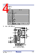
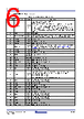
6 / 62 page  R31DS0210EU0106 Rev.1.06 Page 6 May 11, 2026 RC193xx Datasheet 1.3.2 RC19308 Pin Descriptions Table 1. RC19308A/A001 Pin Descriptions Pin Number Pin Name Type Description 1 ZOUTSEL_tri I, SE, PD, PU Input to select differential output impedance. 0 = 85Ω, 1 = 100Ω, M = 34Ω Note: This pin is bi-level on the RC19208 clock multiplexer with an internal pull-down, which results in a default output impedance of 85Ω when left floating. This pin is tri-level on the RC19308 with both internal pull-up and pull-down resistors. On the RC19308, this results in a default output impedance of 34Ω when left floating. This pin must be pulled down or pulled up to select an output impedance of 85Ω or 100Ω, respectively. 2 VDDDIG PWR Digital power. 3 PWRGD_PWRDNb I, SE, PU, PDT Input notifies device to sample latched inputs and start up on first high assertion. Low enters Power Down Mode, subsequent high assertions exit Power Down Mode. 4 CLKIN0 I, DIF True clock input. 5 CLKINb0 I, DIF Complementary clock input. 6 VDDIN0 PWR Power supply for clock input 0. 7 SADR_tri0 I, SE, PD, PU SMBus address bit. This is a tri-level input that works in conjunction with other SADR pins, if present, to decode SMBus Addresses. See the SMBus Address Selection (RC19308) table and refer to the tri-level input thresholds in the electrical tables. 8 CLKIN1 I, DIF True clock input. 9 CLKINb1 I, DIF Complementary clock input. 10 SDATA I/O, SE, OD, PDT Data pin for SMBus interface. 11 SCLK I, SE, PDT Clock pin of SMBus interface. 12 VDDIN1 PWR Power supply for clock input 1. 13 VDDCLK_1 PWR Power supply for clock output bank 1. 14 CLK7 O, DIF True clock output. 15 CLKb7 O, DIF Complementary clock output. 16 OEb7 I, SE, PU, PDT Active low input for enabling output 7. 0 = Enable output, 1 = Disable output. 17 CLKSEL_tri I, SE, PD, PU Input to select differential input clock 0 or differential input clock 1. This input has an internal pull-up and pull-down resistor to bias a floating pin to the mid-point. 0 = CLKIN0 selected for all outputs. 1 = CLKIN1 selected for all outputs. M = CLKIN0 goes to bank 0 and CLKIN1 goes to bank 1. 18 OEb6 I, SE, PU, PDT Active low input for enabling output 6. 0 = Enable output, 1 = Disable output. 19 CLK6 O, DIF True clock output. 20 CLKb6 O, DIF Complementary clock output. 21 VDDCLK_1 PWR Power supply for clock output bank 1. 22 CLK5 O, DIF True clock output. 23 CLKb5 O, DIF Complementary clock output. 24 OEb5 I, SE, PU, PDT Active low input for enabling output 5. 0 = Enable output, 1 = Disable output. 25 OEb4 I, SE, PU, PDT Active low input for enabling output 4. 0 = Enable output, 1 = Disable output. 26 CLK4 O, DIF True clock output. 27 CLKb4 O, DIF Complementary clock output. 28 VDDCLK_1 PWR Power supply for clock output bank 1. |
|
链接网址 |
| ALLDATASHEET是否为您带来帮助? [ DONATE ] |
关于 Alldatasheet | 广告服务 | 联系我们 | 隐私政策 | 数据表链接 | 链接交换 | 制造商名单 All Rights Reserved©Alldatasheet.com |
| Russian : Alldatasheetru.com | Korean : Alldatasheet.co.kr | Spanish : Alldatasheet.es | French : Alldatasheet.fr | Italian : Alldatasheetit.com Portuguese : Alldatasheetpt.com | Polish : Alldatasheet.pl | Vietnamese : Alldatasheet.vn Indian : Alldatasheet.in | Mexican : Alldatasheet.com.mx | British : Alldatasheet.co.uk | New Zealand : Alldatasheet.co.nz |
|
Family Site : ic2ic.com |
icmetro.com |
 Chinese ▼
 English
 Chinese
 German
 Japanese
 Russian
 Korean
 Spanish
 French
 Italian
 Portuguese
 Polish
 Vietnamese
 Indian
 Mexican
 British
 New Zealand